


Analog-to-Digital Converter (S08ADC12V1)
MCF51QE128 MCU Series Reference Manual, Rev. 3
232 Freescale Semiconductor
Get the latest version from freescale.com
11.4.4.4 Power Control
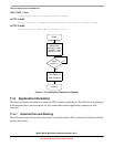
The ADC module remains in its idle state until a conversion is initiated. If ADACK is selected as the
conversion clock source, the ADACK clock generator is also enabled.
Power consumption when active can be reduced by setting ADLPC. This results in a lower maximum
value for f
ADCK
(see the electrical specifications).
11.4.4.5 Sample Time and Total Conversion Time
The total conversion time depends on the sample time (as determined by ADLSMP), the MCU bus
frequency, the conversion mode (8-bit, 10-bit or 12-bit), and the frequency of the conversion clock (f
ADCK
).
After the module becomes active, sampling of the input begins. ADLSMP selects between short (3.5
ADCK cycles) and long (23.5 ADCK cycles) sample times.When sampling is complete, the converter is
isolated from the input channel and a successive approximation algorithm is performed to determine the
digital value of the analog signal. The result of the conversion is transferred to ADCRH and ADCRL upon
completion of the conversion algorithm.
If the bus frequency is less than the f
ADCK
frequency, precise sample time for continuous conversions
cannot be guaranteed when short sample is enabled (ADLSMP=0). If the bus frequency is less than 1/11th
of the f
ADCK
frequency, precise sample time for continuous conversions cannot be guaranteed when long
sample is enabled (ADLSMP=1).
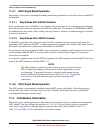
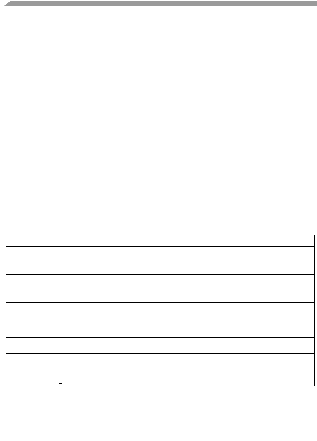
The maximum total conversion time for different conditions is summarized in Table 11-13.
The maximum total conversion time is determined by the clock source chosen and the divide ratio selected.
The clock source is selectable by the ADICLK bits, and the divide ratio is specified by the ADIV bits. For
Table 11-13. Total Conversion Time vs. Control Conditions
Conversion Type ADICLK ADLSMP Max Total Conversion Time
Single or first continuous 8-bit 0x, 10 0 20 ADCK cycles + 5 bus clock cycles
Single or first continuous 10-bit or 12-bit 0x, 10 0 23 ADCK cycles + 5 bus clock cycles
Single or first continuous 8-bit 0x, 10 1 40 ADCK cycles + 5 bus clock cycles
Single or first continuous 10-bit or 12-bit 0x, 10 1 43 ADCK cycles + 5 bus clock cycles
Single or first continuous 8-bit 11 0 5 μs + 20 ADCK + 5 bus clock cycles
Single or first continuous 10-bit or 12-bit 11 0 5 μs + 23 ADCK + 5 bus clock cycles
Single or first continuous 8-bit 11 1 5 μs + 40 ADCK + 5 bus clock cycles
Single or first continuous 10-bit or 12-bit 11 1 5 μs + 43 ADCK + 5 bus clock cycles
Subsequent continuous 8-bit;
f
BUS
> f
ADCK
xx 0 17 ADCK cycles
Subsequent continuous 10-bit or 12-bit;
f
BUS
> f
ADCK
xx 0 20 ADCK cycles
Subsequent continuous 8-bit;
f
BUS
> f
ADCK
/11
xx 1 37 ADCK cycles
Subsequent continuous 10-bit or 12-bit;
f
BUS
> f
ADCK
/11
xx 1 40 ADCK cycles