


MCF51QE128 MCU Series Reference Manual, Rev. 3
20 Freescale Semiconductor
Get the latest version from freescale.com
Section Number Title Page
16.4.4 SPI Status Register (SPIxS) ............................................................................................324
16.4.5 SPI Data Register (SPIxD) .............................................................................................325
16.5 Functional Description ..................................................................................................................325
16.5.1 SPI Clock Formats ..........................................................................................................326
16.5.2 SPI Interrupts ..................................................................................................................328
16.5.3 Mode Fault Detection .....................................................................................................329
Chapter 17
Timer/Pulse-Width Modulator (S08TPMV3)
17.1 Introduction ...................................................................................................................................331
17.1.1 ACMP/TPM Configuration Information ........................................................................331
17.1.2 TPM Clock Gating ..........................................................................................................331
17.1.3 Interrupt Vector ...............................................................................................................331
17.1.4 Features ...........................................................................................................................335
17.1.5 Modes of Operation ........................................................................................................335
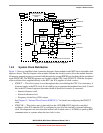
17.1.6 Block Diagram ................................................................................................................336
17.2 Signal Description .........................................................................................................................338
17.2.1 Detailed Signal Descriptions ..........................................................................................338
17.2.1.1 EXTCLK — External Clock Source ............................................................339
17.2.1.2 TPMxCHn — TPM Channel n I/O Pin(s) ....................................................339
17.3 Register Definition ........................................................................................................................341
17.3.1 TPM Status and Control Register (TPMxSC) ................................................................341
17.3.2 TPM Counter Registers (TPMxCNTH:TPMxCNTL) ....................................................342
17.3.3 TPM Counter Modulo Registers (TPMxMODH:TPMxMODL) ....................................343
17.3.4 TPM Channel n Status and Control Register (TPMxCnSC) ..........................................344
17.3.5 TPM Channel Value Registers (TPMxCnVH:TPMxCnVL) ..........................................346
17.4 Functional Description ..................................................................................................................347
17.4.1 Counter ............................................................................................................................347
17.4.1.1 Counter Clock Source ...................................................................................347
17.4.1.2 Counter Overflow and Modulo Reset ...........................................................348
17.4.1.3 Counting Modes ............................................................................................349
17.4.1.4 Manual Counter Reset ..................................................................................349
17.4.2 Channel Mode Selection .................................................................................................349
17.4.2.1 Input Capture Mode ......................................................................................349
17.4.2.2 Output Compare Mode .................................................................................349
17.4.2.3 Edge-Aligned PWM Mode ...........................................................................350
17.4.2.4 Center-Aligned PWM Mode .........................................................................351
17.5 Reset Overview .............................................................................................................................352
17.5.1 General ............................................................................................................................352
17.5.2 Description of Reset Operation .......................................................................................352
17.6 Interrupts .......................................................................................................................................352
17.6.1 General ............................................................................................................................352