


MCF51QE128 MCU Series Reference Manual, Rev. 3
328 Freescale Semiconductor
Get the latest version from freescale.com
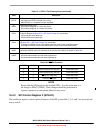
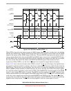
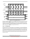
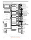
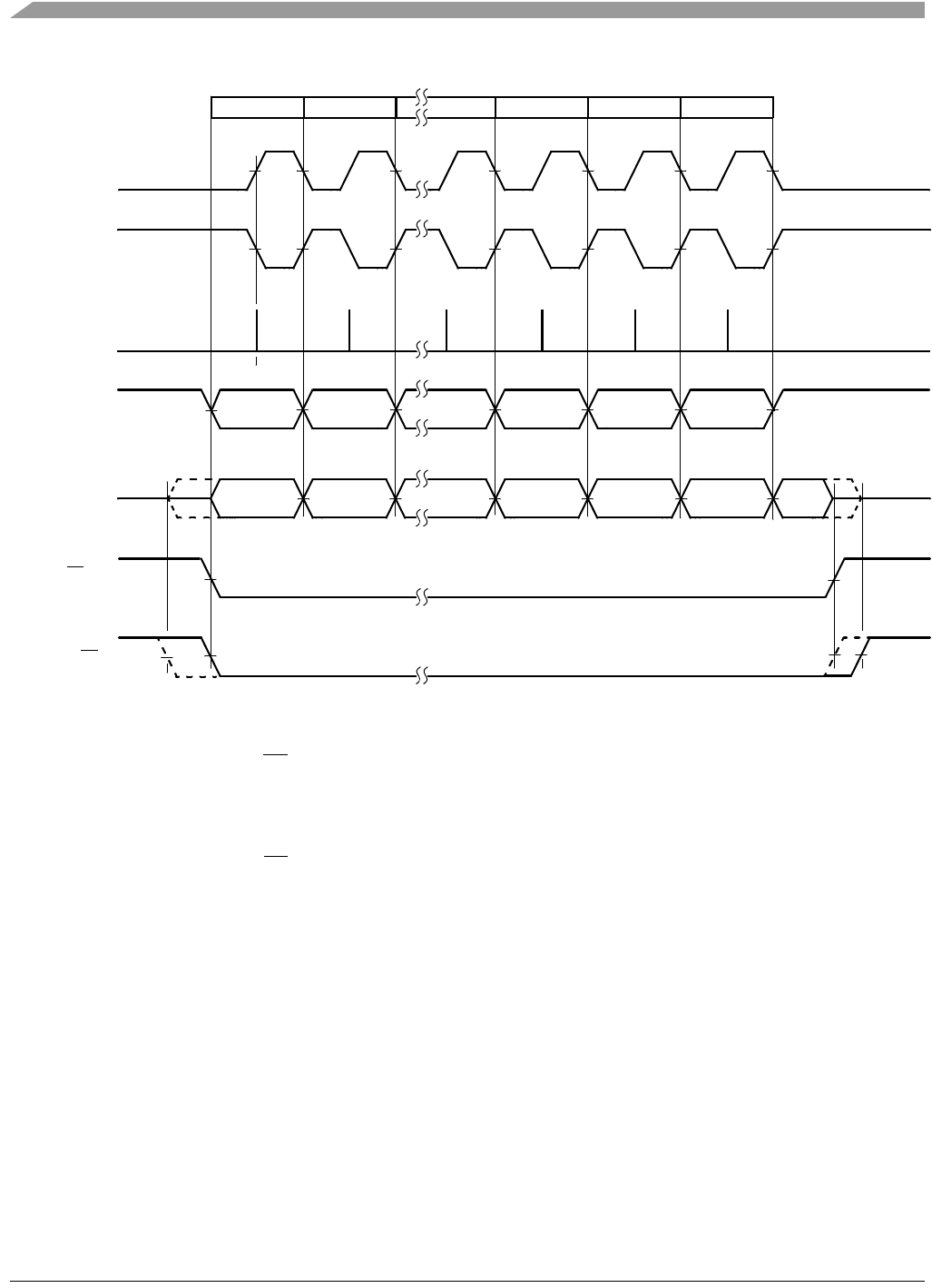
Figure 16-11. SPI Clock Formats (CPHA = 0)
When CPHA is cleared, the slave begins to drive its MISO output with the first data bit value (msb or lsb
depending on LSBFE) when SS asserts. The first SPSCK edge causes the master and the slave to sample
the data bit values on their MISO and MOSI inputs, respectively. At the second SPSCK edge, the SPI
shifter shifts one bit position that shifts in the bit value that was sampled and shifts the second data bit value
out the other end of the shifter to the MOSI and MISO outputs of the master and slave, respectively. When
CPHA is cleared, the slave’s SS input must negate between transfers.
16.5.2 SPI Interrupts
There are three flag bits, two interrupt mask bits, and one interrupt vector associated with the SPI system.
The SPIE bit enables interrupts from the SPI receiver full flag (SPRF) and mode fault flag (MODF). The
SPTIE bit enables interrupts from the SPI transmit buffer empty flag (SPTEF). When one of the flag bits
is set, and the associated interrupt mask bit is set, a hardware interrupt request is sent to the CPU. If the
interrupt mask bits are cleared, software can poll the associated flag bits instead of using interrupts. The
SPI interrupt service routine (ISR) should check the flag bits to determine what event caused the interrupt.
The service routine should also clear the flag bit(s) before returning from the ISR (usually near the
beginning of the ISR).
BIT TIME #
(REFERENCE)
msb FIRST
lsb FIRST
SPSCK
(CPOL = 0)
SPSCK
(CPOL = 1)
SAMPLE IN
(MISO OR MOSI)
MOSI
(MASTER OUT)
MISO
(SLAVE OUT)
SS
OUT
(MASTER)
SS
IN
(SLAVE)
BIT 7
BIT 0
BIT 6
BIT 1
BIT 2
BIT 5
BIT 1
BIT 6
BIT 0
BIT 7
12 67 8...
...
...