RL78/G1A
CHAPTER 30 ELECTRICAL SPECIFICATIONS (G: INDUSTRIAL APPLICATIONS T
A
=
−
40 to +105
°
C)
R01UH0305EJ0200 Rev.2.00 921
Jul 04, 2013
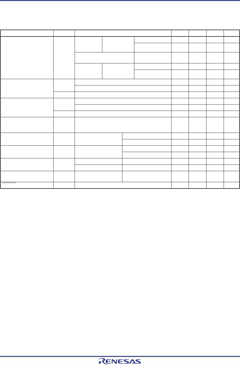
30.4 AC Characteristics
(TA = −40 to +105°C, AVDD ≤ VDD ≤ 3.6 V, 2.4 V ≤ EVDD0 ≤ VDD ≤ 3.6 V, VSS = EVSS0 = 0 V)
Items Symbol Conditions MIN. TYP. MAX. Unit
2.7 V ≤ VDD ≤ 3.6 V 0.03125 1
μ
s Main system
clock (f
MAIN)
operation
HS (high-speed
main) mode
2.4 V ≤ V
DD < 2.7 V 0.0625 1
μ
s
Subsystem clock (fSUB)
operation
2.4 V ≤ VDD ≤ 3.6 V 28.5 30.5 31.3
μ
s
2.7 V ≤ VDD ≤ 3.6 V 0.03125 1
μ
s
Instruction cycle (minimum
instruction execution time)
TCY
In the self
programming
mode
HS (high-speed
main) mode
2.4 V ≤ V
DD < 2.7 V 0.0625 1
μ
s
2.7 V ≤ VDD ≤ 3.6 V 1.0 20.0 MHzfEX
2.4 V ≤ V
DD < 2.7 V 1.0 16.0 MHz
External system clock
frequency
f
EXS 32 35 kHz
2.7 V ≤ VDD ≤ 3.6 V 24 ns tEXH, tEXL
2.4 V ≤ VDD < 2.7 V 30 ns
External system clock input
high-level width, low-level
width
t
EXHS, tEXLS 13.7
μ
s
TI00, TI01, TI03 to TI07
input high-level width,
low-level width
tTIH, tTIL 1/fMCK+10 ns
Note
2.7 V ≤ EVDD0 ≤ 3.6 V 8 MHzTO00, TO01, TO03 to TO07
output frequency
fTO
HS (high-speed main)
mode
2.4 V ≤ EV
DD0 < 2.7 V 4 MHz
2.7 V ≤ EVDD0 ≤ 3.6 V 8 MHzPCLBUZ0, PCLBUZ1
output frequency
fPCL HS (high-speed main)
mode
2.4 V ≤ EV
DD0 < 2.7 V 4 MHz
INTP0 2.4 V ≤ VDD ≤ 3.6 V 1
μ
s Interrupt input high-level
width, low-level width
tINTH, tINTL
INTP1 to INTP11 2.4 V ≤ EV
DD0 ≤ 3.6 V 1
μ
s
Key interrupt input high-
level width, low-level width
tKR KR0 to KR9 2.4 V ≤ EVDD0 ≤ 3.6 V,
2.4 V ≤ AV
DD0 ≤ 3.6 V
250 ns
RESET low-level width tRSL 10
μ
s
Note The following conditions are required for low-voltage interface when EVDD0 < VDD.
2.4 V ≤ EV
DD0 < 2.7 V : MIN. 125 ns
Remark f
MCK: Timer array unit operation clock frequency
(Operation clock to be set by the CKS0n bit of timer clock select register 0 (TPS0) and timer mode register 0n
(TMR0n). n: Channel number (n = 0 to 7))


