RL78/G1A CHAPTER 26 ON-CHIP DEBUG FUNCTION
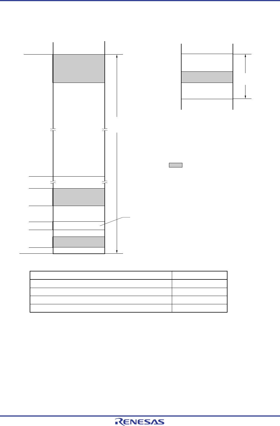
Figure 26-2. Memory Spaces Where Debug Monitor Programs Are Allocated
(512 bytes or
256 bytes
Note 2
)
: Area used for on-chip debugging
Note 1
Note 3
Code flash memory
Use prohibited
Internal RAM
Code flash
area
Mirror area
SFR area
Debug monitor area
(2 bytes)
Debug monitor area
(10 bytes)
Security ID area
(10 bytes)
On-chip debug option byte area
(1 byte)
Stack area for debugging
(4 bytes)
Note 4
01000H
000D8H
000CEH
000C4H
000C3H
00002H
00000H
Internal RAM
area
Notes 1. Address differs depending on products as follows.
Address of Note 1 Products (code flash memory capacity)
R5F10ExA (x = 8, B, G) 03FFFH
R5F10ExC (x = 8, B, G, L) 07FFFH
R5F10ExD (x = 8, B, G, L) 0BFFFH
R5F10ExE (x = 8, B, G, L) 0FFFFH
2. When real-time RAM monitor (RRM) function and dynamic memory modification (DMM) function are not
used, it is 256 bytes.
3. In debugging, reset vector is rewritten to address allocated to a monitor program.
4. Since this area is allocated immediately before the stack area, the address of this area varies depending on
the stack increase and decrease. That is, 4 extra bytes are consumed for the stack area used.
When using self-programming, 12 extra bytes are consumed for the stack area used.
R01UH0305EJ0200 Rev.2.00 826
Jul 04, 2013


