RL78/G1A CHAPTER 12 SERIAL ARRAY UNIT
R01UH0305EJ0200 Rev.2.00 430
Jul 04, 2013
12.3.16 Noise filter enable register 0 (NFEN0)
The NFEN0 register is used to set whether the noise filter can be used for the input signal from the serial data input pin
to each channel.
Disable the noise filter of the pin used for CSI or simplified I
2
C communication, by clearing the corresponding bit of this
register to 0.
Enable the noise filter of the pin used for UART communication, by setting the corresponding bit of this register to 1.
When the noise filter is enabled, after synchronization is performed with the operation clock (f
MCK) of the target channel,
2-clock match detection is performed. When the noise filter is OFF, only synchronization is performed with the operation
clock (f
MCK) of the target channel.
The NFEN0 register can be set by a 1-bit or 8-bit memory manipulation instruction.
Reset signal generation clears the NFEN0 register to 00H.
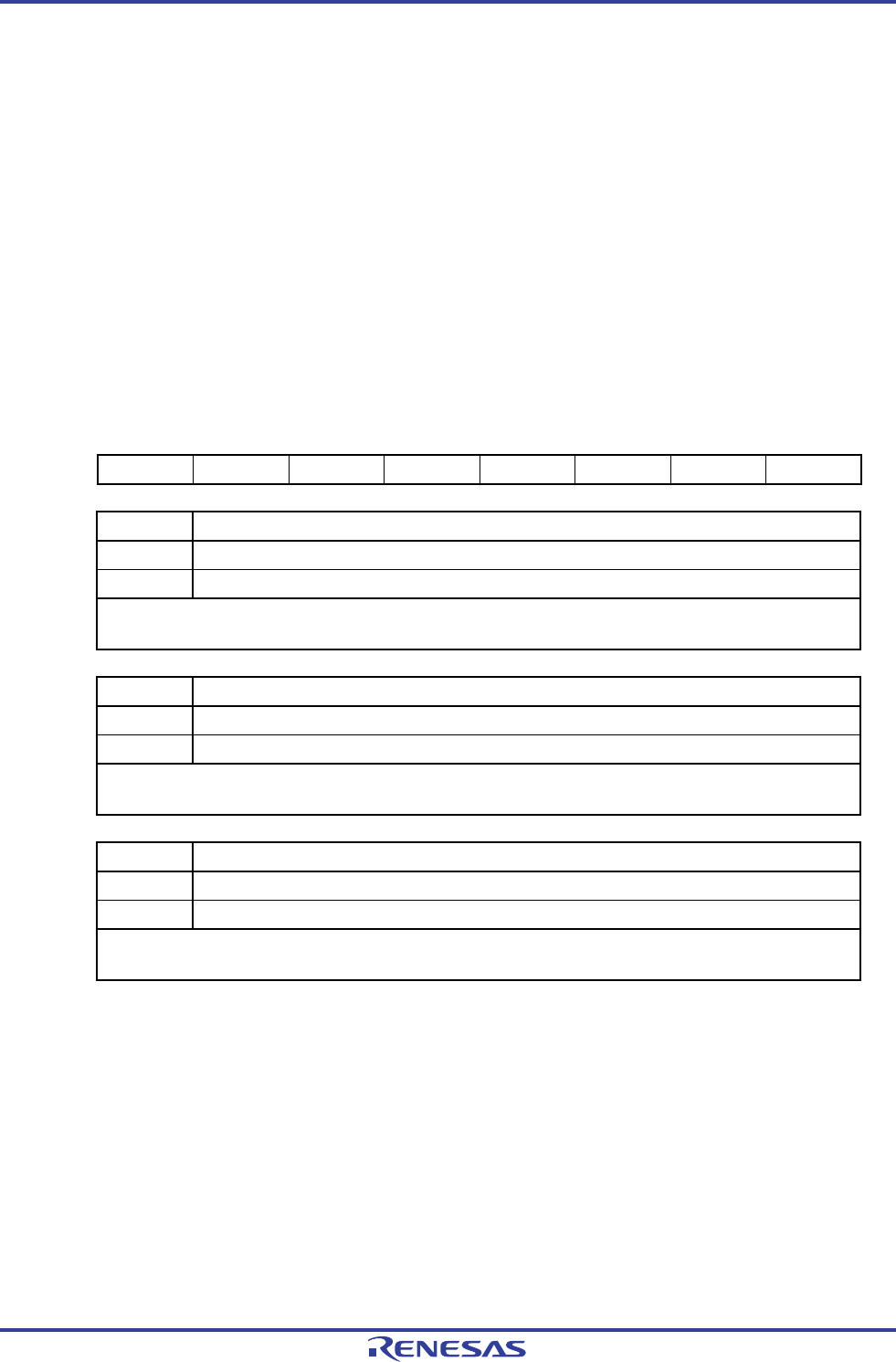
Figure 12-21. Format of Noise Filter Enable Register 0 (NFEN0)
Address: F0070H After reset: 00H R/W
Symbol 7 6 5 4 3 2 1 0
NFEN0 0 0 0 SNFEN20 0 SNFEN10 0 SNFEN00
SNFEN20 Use of noise filter of RXD2 pin (RXD2/SDA20/SI20/P14)
0 Noise filter OFF
1 Noise filter ON
Set SNFEN20 to 1 to use the RXD2 pin.
Clear SNFEN20 to 0 to use the other than RxD2 pin.
SNFEN10 Use of noise filter of RXD1 pin (RXD1/ANI16/SI10/SDA10/P03)
0 Noise filter OFF
1 Noise filter ON
Set the SNFEN10 bit to 1 to use the RXD1 pin.
Clear the SNFEN10 bit to 0 to use the other than RxD1 pin.
SNFEN00 Use of noise filter of RXD0 pin (RXD0/TOOLRXD/SDA00/SI00/P11)
0 Noise filter OFF
1 Noise filter ON
Set the SNFEN00 bit to 1 to use the RXD0 pin.
Clear the SNFEN00 bit to 0 to use the other than RxD0 pin.
Caution Be sure to clear bits 7 to 5, 3, and 1 to “0”.
<R>


