RL78/G1A CHAPTER 29 ELECTRICAL SPECIFICATIONS (T
A = −40 to +85°C)
R01UH0305EJ0200 Rev.2.00 866
Jul 04, 2013
Note The following conditions are required for low-voltage interface when EVDD0 < VDD.
1.8 V ≤ EVDD0 < 2.7 V : MIN. 125 ns
1.6 V ≤ EV
DD0 < 1.8 V : MIN. 250 ns
Remark f
MCK: Timer array unit operation clock frequency
(Operation clock to be set by the CKS0n bit of timer clock select register 0 (TPS0) and timer mode register 0n
(TMR0n). n: Channel number (n = 0 to 7))
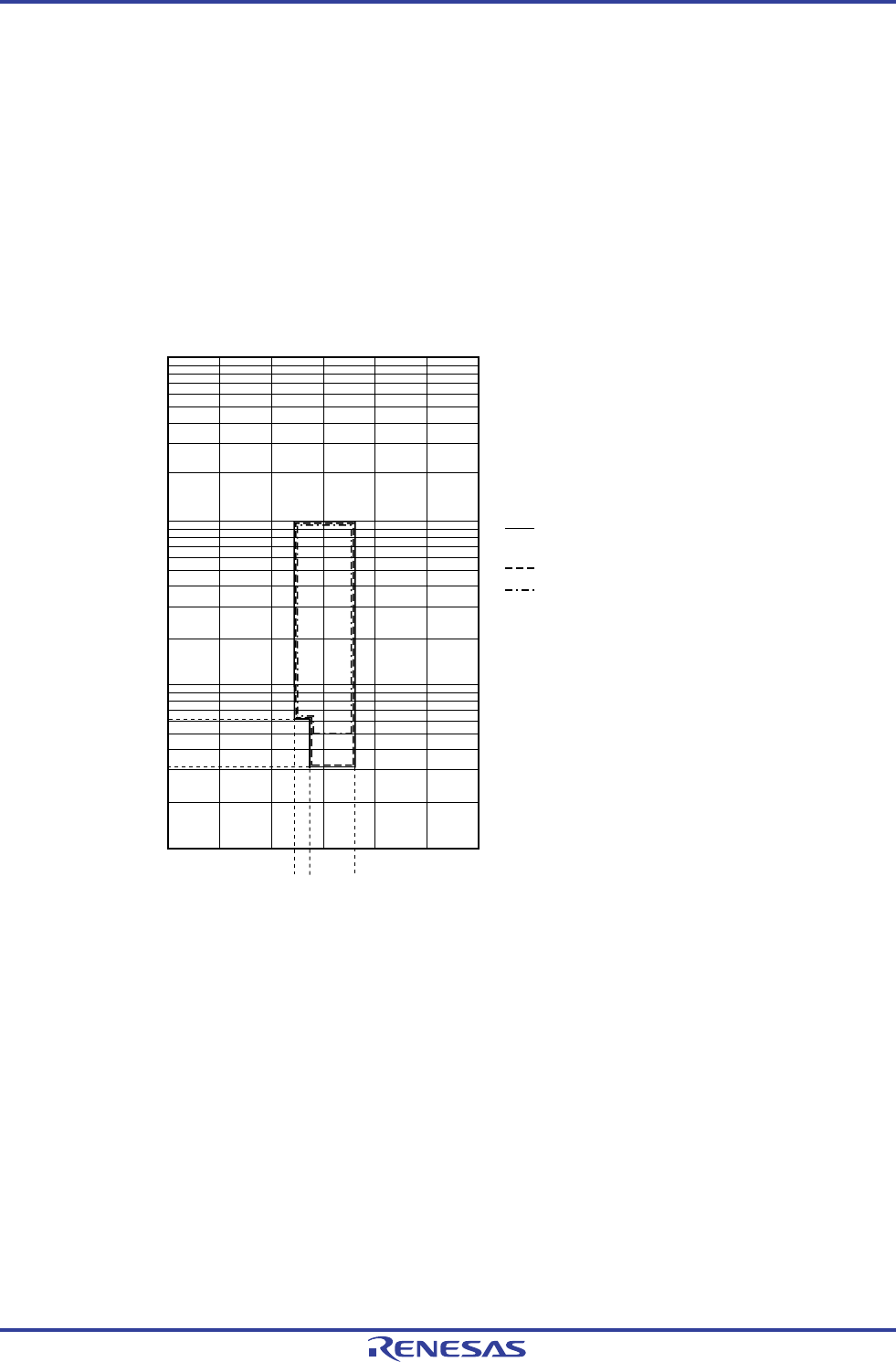
Minimum Instruction Execution Time during Main System Clock Operation
T
CY vs VDD (HS (high-speed main) mode)
1.0
0.1
0
10
1.0 2.0 3.0 4.0 5.0 6.0
3.6
2.7
0.01
2.4
0.03125
0.0625
0.05
Cycle time TCY [μs]
Supply voltage VDD [V]
When the high-speed on-chip oscillator
clock is selected
During self programming
When high-speed system clock is selected
<R>


