RL78/G1A CHAPTER 21 VOLTAGE DETECTOR
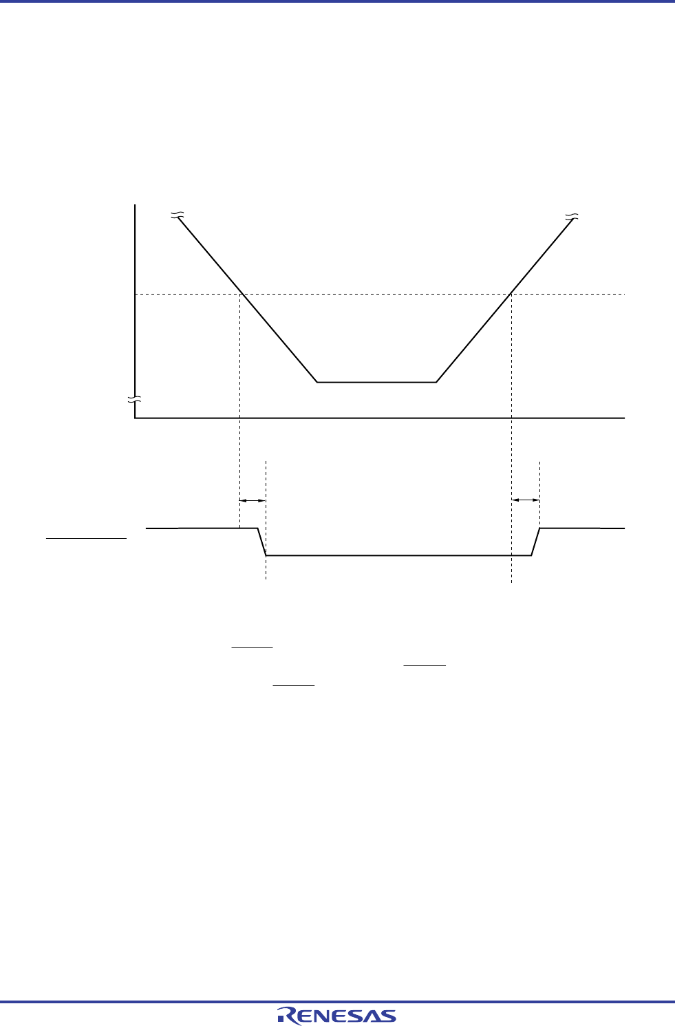
(2) Delay from the time LVD reset source is generated until the time LVD reset has been generated or released
There is some delay from the time supply voltage (VDD) < LVD detection voltage (VLVD) until the time LVD reset has
been generated.
In the same way, there is also some delay from the time LVD detection voltage (V
LVD) ≤ supply voltage (VDD) until
the time LVD reset has been released (see Figure 21-10).
Figure 21-10. Delay from the Time LVD Reset Source Is Generated Until the Time LVD Reset has Been Generated or
Released
V
LVD
Supply voltage (V
DD
)
LVD reset signal
<1>
Time
<1>
<1>: Detection delay (300
μ
s (MAX.))
<R>
(3) Power on when LVD is off
Use the external rest input via the RESET pin when the LVD is off.
For an external reset, input a low level for 10
μ
s or more to the RESET pin. To perform an external reset upon
power application, input a low level to the RESET pin, turn power on, continue to input a low level to the pin for 10
μ
s or more within the operating voltage range shown in 29.4 or 30.4 AC Characteristics, and then input a high
level to the pin.
(4) Operating voltage fall when LVD is off or LVD interrupt mode is selected
<R>
When the operating voltage falls with the LVD is off or with the LVD interrupt mode is selected, this LSI should be
placed in the STOP mode, or placed in the reset state by controlling the externally input reset signal, before the
voltage falls below the operating voltage range defined in 29.4 or 30.4 AC characteristics. When restarting the
operation, make sure that the operation voltage has returned within the range of operation.
R01UH0305EJ0200 Rev.2.00 771
Jul 04, 2013


