RL78/G1A CHAPTER 17 KEY INTERRUPT FUNCTION
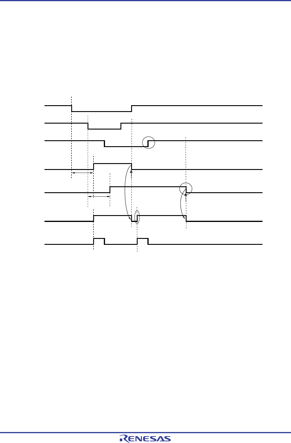
The operation when a valid edge is input to the KR6 to KR9 pins without generating a key interrupt (INTKR) is shown in
Figure 17-11 below. A falling edge is also input to the KR1 and KR6 pins after a falling edge was input to the KR0 pin
(when KREG = 0). The KR1 pin becomes high level when the KRF0 bit is cleared, but because the KRF1 bit is set, a key
interrupt (INTKR) is generated one clock (f
CLK) after the KRF0 bit is cleared (<1> in the figure). Also, because the KR6 pin
was high level (<3> in the figure) before the KRF1 bit was cleared (<2> in the figure) a key interrupt (INTKR) is not
generated for the KR6 pin.
Figure 17-11. Operation When an INTKR Signal Is Not Generated upon Input of a Valid Edge to KR6 to KR9
(When KRMD = 1 and KREG = 0)
KR0
KR1
KR6
KRF0
KRF1
INTKR
KRIF
Note 1
Delay
time
Note 1
Delay
time
Note 2Note 2
Clear
Clear
Cleared by software
<2>
<1>
Cleared by software
<3>
Notes 1. The maximum delay time is the maximum value of the high-level width and low-level width of the key
interrupt input (see 29.4 AC Characteristics and 30.4 AC Characteristics for details).
2. Acknowledgment of vectored interrupt request or bit cleared by software
Remark f
CLK: CPU/peripheral hardware clock frequency
R01UH0305EJ0200 Rev.2.00 725
Jul 04, 2013


