RL78/G1A CHAPTER 11 A/D CONVERTER
R01UH0305EJ0200 Rev.2.00 397
Jul 04, 2013
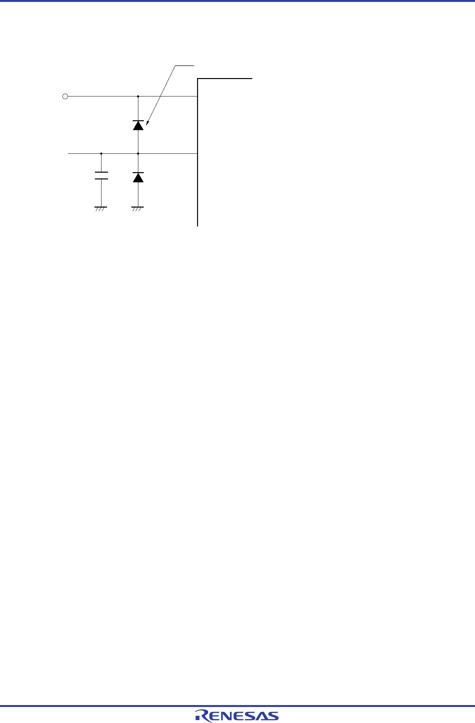
Figure 11-44. Analog Input Pin Connection
AV
REFP
, or AV
DD
ANI0 to ANI12, ANI16 to ANI30
Reference
voltage
input
C = 10 pF to 0.1 μF
If there is a possibility that noise equal to or higher than AV
REFP
, and AV
DD
or equal to or lower than AV
REFM
, and AV
SS
, may enter, clamp
with a diode with a small V
F
value (0.3 V or lower).
(5) Analog input (ANIn) pins
<1> ANI0 to ANI12 pins (high-accuracy channel) are also used as P20 to P27, and P150 to P154 pins.
When A/D conversion is performed with any of the high-accuracy channel (ANI0 to ANI12) pins selected, do not
change the output value P20 to P27, and P150 to P154 while conversion is in progress; otherwise the
conversion accuracy may be degraded.
<2> If a pin adjacent to the pin whose value is being A/D converted is used as a digital I/O port pin, the A/D
conversion value might differ from the expected value due to coupling noise. To prevent coupling noise, make
sure that pulses whose voltage suddenly change, such as digital pulses, are not input or output to a pin
adjacent to the pin whose value is being A/D converted.
(6) Input impedance of analog input (ANIn) pins
This A/D converter charges a sampling capacitor for sampling during sampling time.
Therefore, only a leakage current flows when sampling is not in progress, and a current that charges the capacitor
flows during sampling. Consequently, the input impedance fluctuates depending on whether sampling is in progress,
and on the other states.
However, in order to perform sampling accurately, the output impedance of the analog input source should be 1 kΩ or
lower. If it is not possible to keep the output impedance below this level, it is recommended to either extend the
sampling time or connect a capacitor of about 0.1
μ
F to the ANI0 to ANI12 and ANI16 to ANI30 pins. (See Figure
11-44 for details.)
Also, if the ADCS bit is set to 0 or a reconversion is started during A/D conversion, the sampling capacitor will be
insufficiently charged. This means that charging will start with an undefined conversion voltage from the next
conversion in the case of setting the ADCS bit to 0, or from the current conversion in the case of starting a
reconversion.
To ensure that the capacitor is fully charged, therefore, either reduce the output impedance of the analog input source
or specify a sufficiently long sampling time, irrespective of the analog signal voltage variation.


