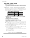
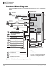
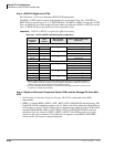
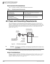
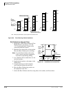
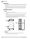
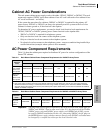
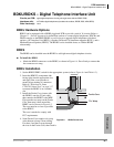
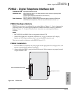
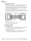
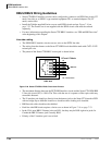
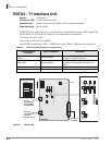
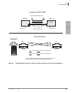
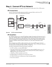
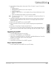
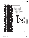
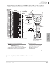
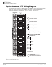
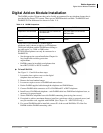
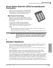
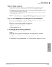
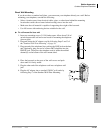
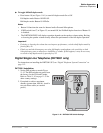
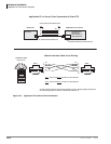
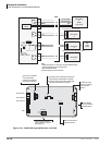
ISDN Interfaces
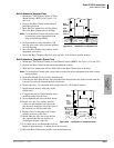
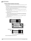
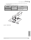
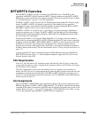
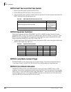
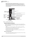
RBSU/RBSS Interface Units
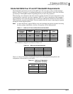
Strata CTX I&M 06/04 7-19
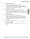
ISDN Interfaces
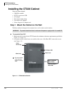
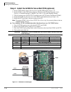
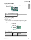
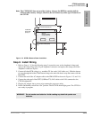
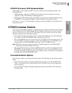
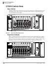
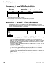
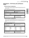
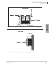
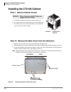
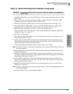
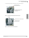
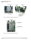
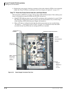
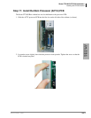
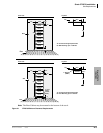
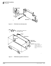
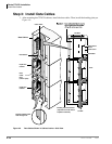
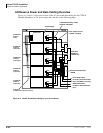
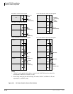
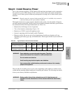
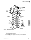
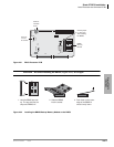
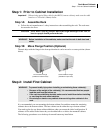
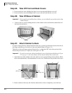
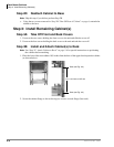
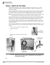
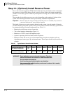
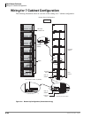
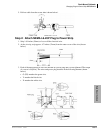
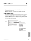
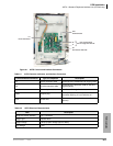
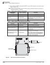
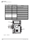
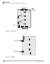
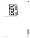
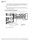
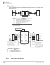
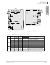
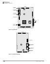
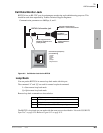
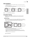
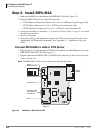
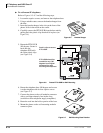
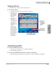
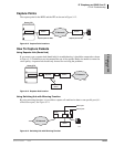
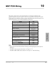
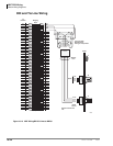
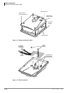
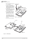
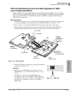
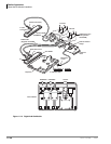
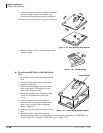
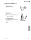
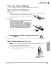
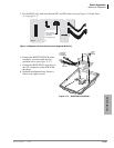
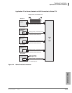
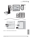
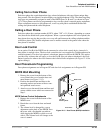
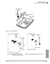
Step 6: Install RBSU/RBSS PCBs into Cabinet
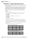
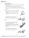
After setting the switches and jumpers and installing the plug-on PCBs as described in the
preceding paragraphs, the RBSU/RBSS PCBs can be installed in the appropriate cabinet slots.
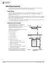
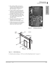
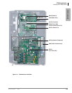
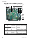
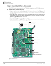
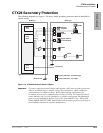
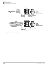
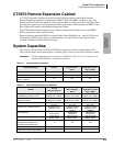
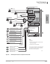
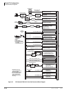
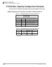
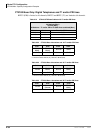
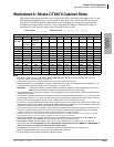
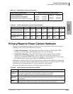
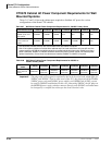
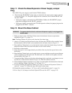
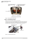
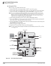
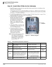
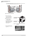
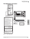
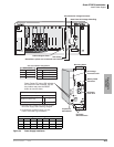
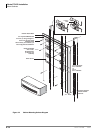
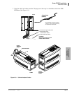
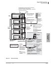
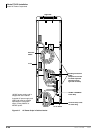
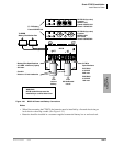
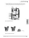
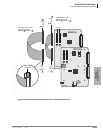
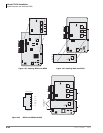
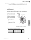
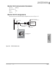
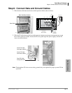
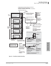
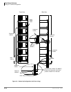
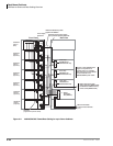
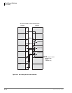
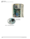
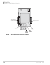
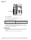
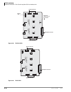
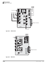
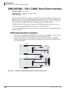
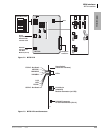
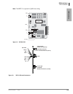
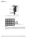
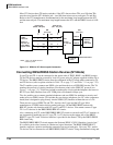
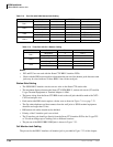
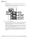
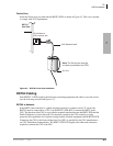
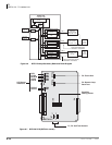
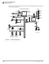
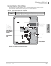
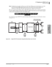
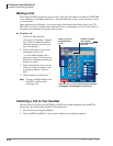
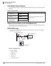
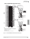
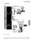
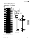
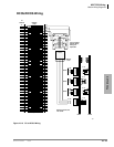
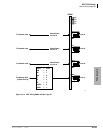
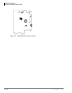
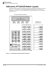
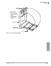
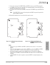
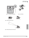
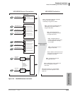
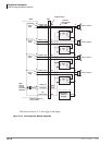
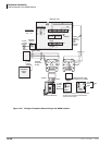
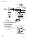
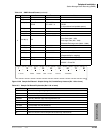
Refer to RBSU/RBSS Capacity and Cabinet Slot Information on Figure 7-14. After the RBSU/
RBSS is installed in the Strata CTX cabinet, the status LEDs and connecting jacks are positioned
as shown in Figure 7-14.
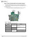
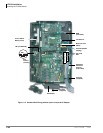
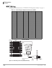
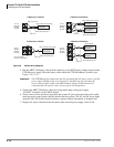
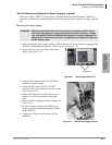
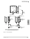
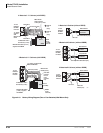
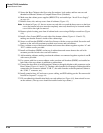
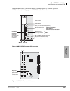
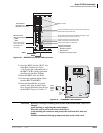
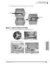
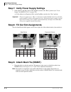
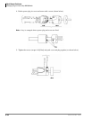
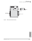
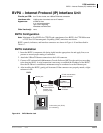
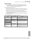
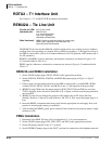
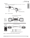
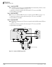
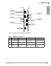
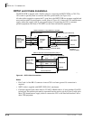
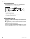
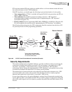
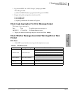
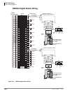
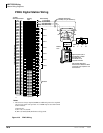
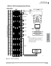
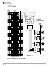
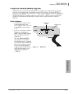
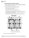
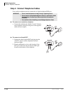
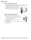
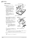
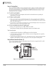
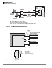
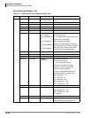
Modular Jack Pin Configurations
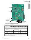
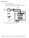
BRI (S/T) Circuit Jack (TE or NT Mode)
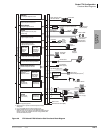
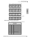
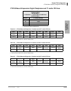
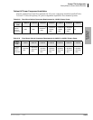
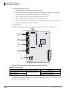
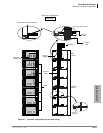
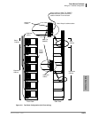
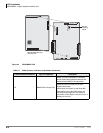
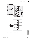
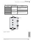
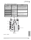
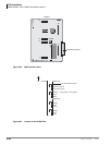
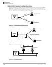
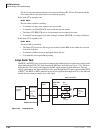
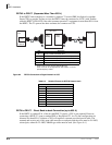
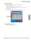
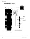
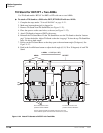
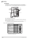
The RBSU and RBSU/RBSS BRI circuit jack is a shielded RJ45 (8-pin modular) with Transmit
(Tx) and Receive (Rx) pin numbers as shown in Figure 7-14. The Tx and Rx pin numbers change
when the BRI circuit is configured with RBSU and RBSU/RBSS option switches for TE or NT
(Tables 7-8 and 7-14). If the R40S is installed on the RBSU, the PS-1 voltage is carried on the Tx/
Rx wires with polarity. (See Table 7-10).
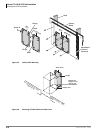
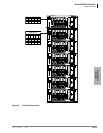
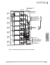
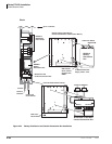
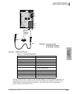
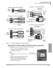
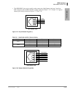
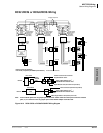
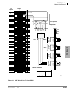
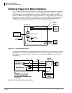
The position of the RBSU BRI and RBSU/RBSS circuit jacks are shown in Figures 7-14 and 7-15
respectively.
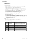
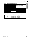
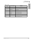
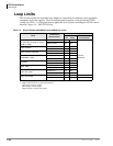
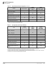
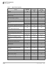
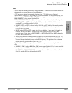
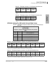
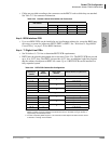
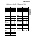
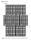
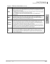
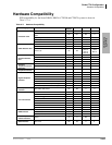
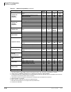
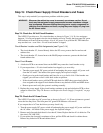
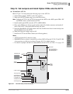
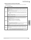
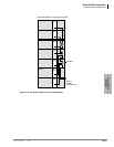
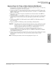
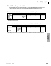
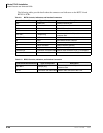
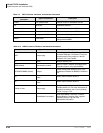
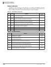
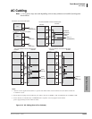
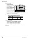
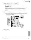
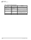
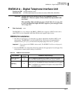
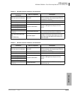
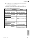
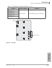
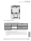
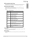
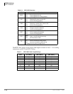
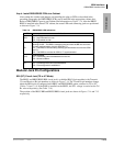
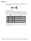
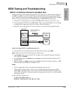
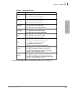
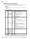
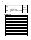
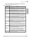
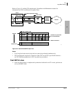
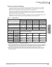
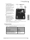
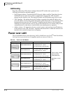
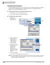
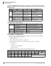
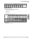
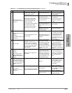
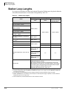
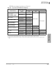
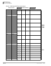
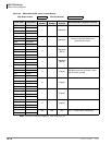
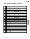
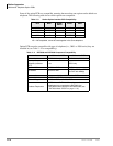
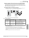
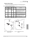
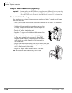
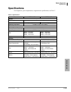
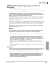
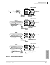
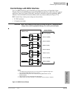
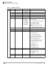
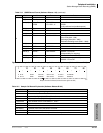
Table 7-9 RBSU/RBSS LED Indications
LED Indication
BSY
Circuit Busy
On – Any B-channel is in use.
Off – B-channels are idle.
TS
Timing Source
Blinking On/Off – The RBSU is extracting the clock from the BRI line and is the
Primary synchronization circuit for ISDN and T1.
On – The RBSU is the secondary (backup) synchronization circuit for the ISDN
and T1.
Off – The RBSU is not used for ISDN or T1 synchronization.
LOS
Loss of Signal
On – Clock timing cannot be detected from the line.
Off – Normal condition.
FS
Frame Alignment Alarm
On – Frame alignment cannot be established.
Off – Frame alignment is established.