


RL78/G1A APPENDIX A REVISION HISTORY
(2/8)
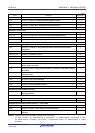
Edition Description Chapter
Addition of remark to 4.3.9 Global digital input disable register (GDIDIS)
Modification of description to 4.3.10 Global analog input disable register (GAIDIS)
Modification of description in 4.4.1 (2) Input mode and 4.4.3 (2) Input mode
Addition of description to 4.4.4 (2) Setting procedure when using I/O pins of IIC00,
IIC10, and IIC20 functions
Addition of caution to 4.5 Settings of Port Mode Register, and Output Latch When
Using Alternate Function
Addition of 4.6.2 Notes on specifying the pin settings
CHAPTER 4 PORT
FUNCTIONS
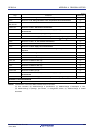
Addition of 5.1 (1) <2> High-speed on-chip oscillator
Modification of Figure 5-1. Block Diagram of Clock Generator
Modification of caution 1 and addition of cautions 4 to 6 to Figure 5-2. Format of
Clock Operation Mode Control Register (CMC)
Modification of cautions 1 to 3 in Figure 5-9. Format of High-speed On-chip
Oscillator Frequency Select Register (HOCODIV)
Modification of note 3 in Figure 5-14. Clock Generator Operation When Power
Supply Voltage Is Turned On
Addition of description to 5.6.2 Example of setting X1 oscillation clock
Addition of description to Figure 5-15. CPU Clock Status Transition Diagram
Modification of Table 5-3. CPU Clock Transition and SFR Register Setting Examples
Modification and deletion of description in Table 5-4. Changing CPU Clock
Modification of remark 2 to 5.6.6 Time required for switchover of CPU clock and
system clock
Addition of 5.7 Recommended Oscillator Constants
CHAPTER 5 CLOCK
GENERATOR
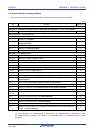
Modification of description in 6.1.1 (7) Delay counter
Modification of caution in 6.1.2 (3) Multiple PWM (Pulse Width Modulation) output
Modification of Figure 6-2. Internal Block Diagram of Channels of Timer Array Unit
0, 2, 4, 6
Addition of Figures 6-3 to 6-6
Modification of Table 6-3. Timer Count Register mn (TCRmn) Read Value in Various
Operation Modes
Modification of note and remark 2 and addition of caution to Figure 6-11. Format of
Timer Clock Select register m (TPSm)
Modification of Figure 6-12. Format of Timer Mode Register mn (TMRmn)
Modification of description in Figure 6-18. Format of Timer Output Enable register m (TOEm)
Modification of description in 6.5.1 (1) When operation clock (fMCK) specified by the
CKSmn0 and CKSmn1 bits is selected (CCSmn = 0)
Modification of description in Table 6-6. Operations from Count Operation Enabled
State to Timer count Register mn (TCRmn) Count Start
Addition of title and remark to 6.5.3 Operation of counter
Rev.0.03
Modification of description, remark and addition note to Figure 6-29. Start Timing (In
Capture Mode : Input Pulse Interval Measurement)
CHAPTER 6 TIMER
ARRAY UNIT
R01UH0305EJ0200 Rev.2.00 975
Jul 04, 2013