


RL78/G1A
CHAPTER 30 ELECTRICAL SPECIFICATIONS (G: INDUSTRIAL APPLICATIONS T
A
=
−
40 to +105
°
C)
R01UH0305EJ0200 Rev.2.00 927
Jul 04, 2013
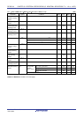
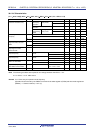
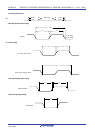
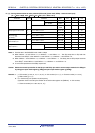
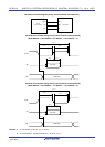
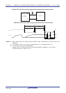
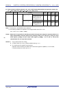
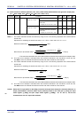
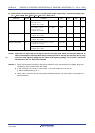
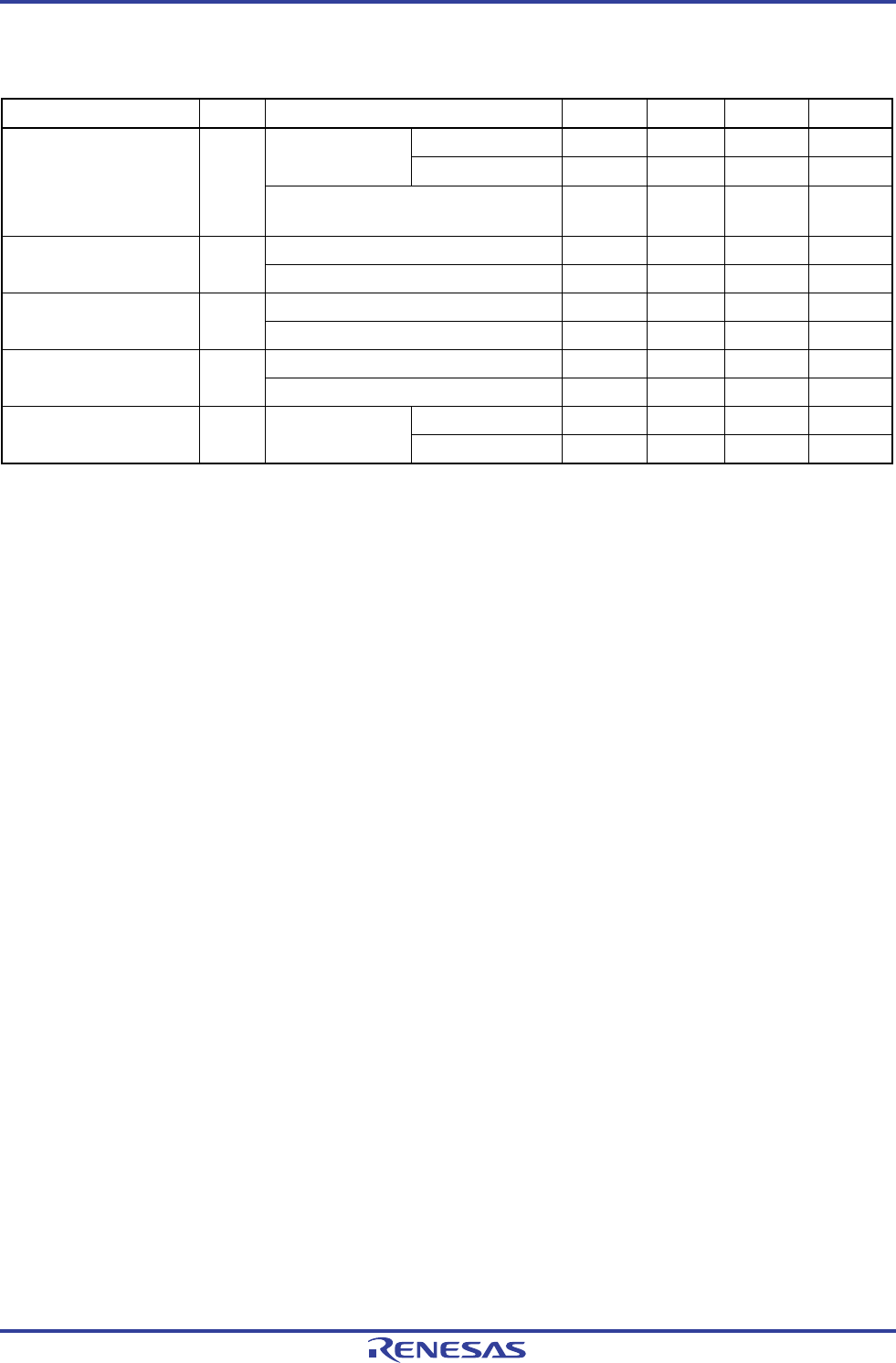
(3) During communication at same potential (CSI mode) (slave mode, SCKp... external clock input)
(TA = −40 to +105°C, 2.4 V ≤ EVDD0 ≤ VDD ≤ 3.6 V, VSS = EVSS0 = 0 V)
Parameter Symbol Conditions MIN. TYP. MAX. Unit
16 MHz < fMCK 16/fMCK ns 2.7 V ≤ EVDD0 ≤ 3.6 V
fMCK ≤ 16 MHz
12/fMCK ns
SCKp cycle time
Note 1
tKCY2
2.4 V ≤ EV
DD0 ≤ 3.6 V
12/f
MCK and
1000
ns
2.7 V ≤ EVDD0 ≤ 3.6 V tKCY2/2−14 ns SCKp high-/low-level width
t
KH2,
t
KL2
2.4 V ≤ EV
DD0 ≤ 3.6 V tKCY2/2−16 ns
2.7 V ≤ EVDD0 ≤ 3.6 V
1/f
MCK + 40
ns
SIp setup time
(to SCKp↑)
Note 2
t
SIK2
2.4 V ≤ EV
DD0 ≤ 3.6 V
1/f
MCK + 60
ns
2.7 V ≤ EVDD0 ≤ 3.6 V 1/fMCK+62 ns
SIp hold time
(from SCKp↑)
Note 2
t
KSI2
2.4 V ≤ EV
DD0 ≤ 3.6 V 1/fMCK+62 ns
2.7 V ≤ EVDD0 ≤ 3.6 V 2/fMCK+66 ns
Delay time from SCKp↓ to
SOp output
Note 3
t
KSO2 C = 30 pF
Note 4
2.4 V ≤ EV
DD0 ≤ 3.6 V 2/fMCK+113 ns
Notes 1. Transfer rate in the SNOOZE mode : MAX. 1 Mbps
2. When DAPmn = 0 and CKPmn = 0, or DAPmn = 1 and CKPmn = 1. The SIp setup time or SIp hold time
becomes “from SCKp↓” when DAPmn = 0 and CKPmn = 1, or DAPmn = 1 and CKPmn = 0.
3. When DAPmn = 0 and CKPmn = 0, or DAPmn = 1 and CKPmn = 1. The delay time to SOp output becomes
“from SCKp↑” when DAPmn = 0 and CKPmn = 1, or DAPmn = 1 and CKPmn = 0.
4. C is the load capacitance of the SOp output lines.
Caution Select the normal input buffer for the SIp pin and SCKp pin and the normal output mode for the SOp pin
by using port input mode register g (PIMg) and port output mode register g (POMg).
Remarks 1. p: CSI number (p = 00, 01, 10, 11, 20, 21), m: Unit number (m = 0, 1), n: Channel number (n = 0 to 3),
g: PIM number (g = 0, 1)
2. f
MCK: Serial array unit operation clock frequency
(Operation clock to be set by the CKSmn bit of serial mode register mn (SMRmn). m: Unit number,
n: Channel number (mn = 00 to 03, 10, 11))
<R>