


RL78/G1A
CHAPTER 30 ELECTRICAL SPECIFICATIONS (G: INDUSTRIAL APPLICATIONS T
A
=
−
40 to +105
°
C)
R01UH0305EJ0200 Rev.2.00 948
Jul 04, 2013
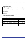
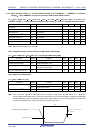
(5) When reference voltage (+) = Internal reference voltage (1.45 V) (ADREFP1 = 1, ADREFP0 = 0), reference
voltage (−) = AVSS (ADREFM = 0), target for conversion: ANI0 to ANI12, ANI16 to ANI30
(T
A = −40 to +105°C, 2.4 V ≤ VDD ≤ 3.6 V, 2.4 V ≤ EVDD ≤ VDD, 2.4 V ≤ AVDD ≤ VDD, VSS = EVSS0 = 0 V, AVSS = 0 V,
Reference voltage (+) = Internal reference voltage, Reference voltage (−) = AV
SS = 0 V, HS (high-speed main) mode)
Parameter Symbol Conditions MIN. TYP. MAX. Unit
Resolution RES 8 bit
Conversion time tCONV 8-bit resolution 16.0
μ
s
Zero-scale error
Note
EZS 8-bit resolution ±4.0 LSB
Integral linearity error
Note
ILE 8-bit resolution ±2.0 LSB
Differential linearity error
Note
DLE 8-bit resolution ±2.5 LSB
Reference voltage (+) AVREF(+) = Internal reference voltage (VBGR) 1.38 1.45 1.50 V
Analog input voltage VAIN 0 VBGR V
Note Excludes quantization error (±1/2 LSB).
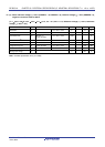
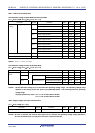
30.6.2 Temperature sensor, internal reference voltage output characteristics
(T
A = −40 to +105°C, 2.4 V ≤ VDD ≤ 3.6 V, VSS = 0 V, HS (high-speed main) mode)
Parameter Symbol Conditions MIN. TYP. MAX. Unit
Temperature sensor output voltage VTMPS25 Setting ADS register = 80H, TA = +25°C 1.05 V
Internal reference voltage VBGR Setting ADS register = 81H 1.38 1.45 1.5 V
Temperature coefficient FVTMPS
Temperature sensor output voltage that
depends on the temperature
−3.6 mV/°C
Operation stabilization wait time tAMP 10
μ
s
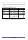
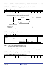
30.6.3 POR circuit characteristics
(T
A = −40 to +105°C, VSS = 0 V)
Parameter Symbol Conditions MIN. TYP. MAX. Unit
VPOR Power supply rise time 1.45 1.51 1.57 V Detection voltage
V
PDR Power supply fall time 1.44 1.50 1.56 V
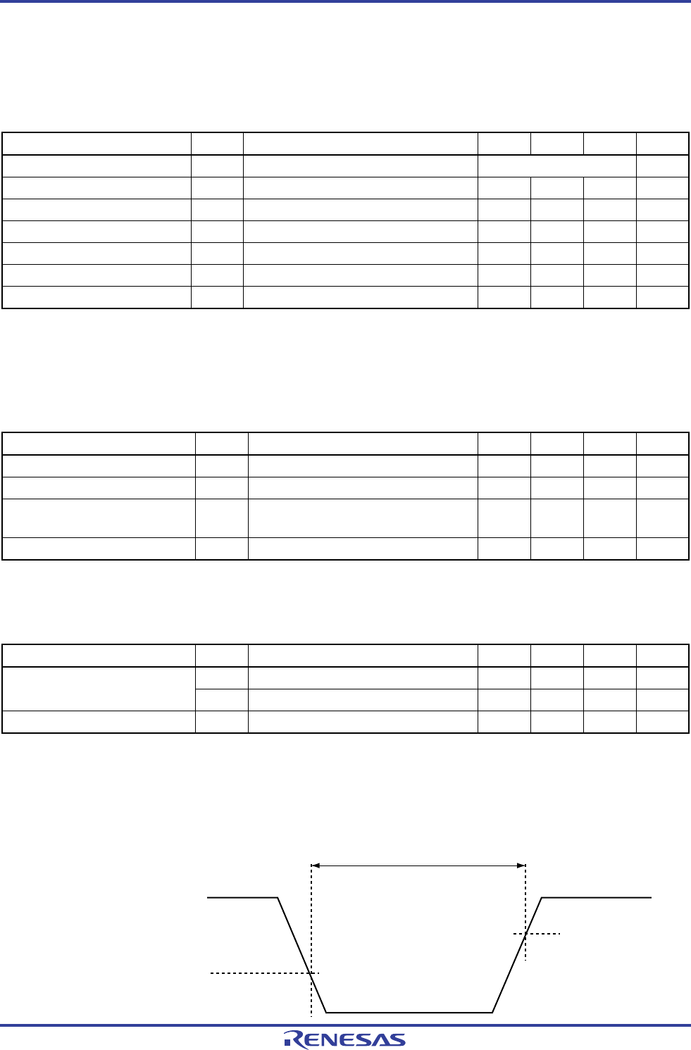
Minimum pulse width
Note
TPW 300
μ
s
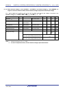
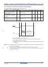
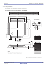
Note This is the time required for the POR circuit to execute a reset when V
DD falls below VPDR. When the
microcontroller enters STOP mode or if the main system clock (f
MAIN) has been stopped by setting bit 0 (HIOSTOP)
and bit 7 (MSTOP) of the clock operation status control register (CSC), this is the time required for the POR circuit
to execute a reset before V
DD rises to VPOR after having fallen below 0.7 V.
V
POR
T
PW
Power supply voltage (V
DD
)
V
POR
or 0.7 V
<R>