


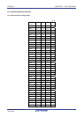
RL78/G1A CHAPTER 2 PIN FUNCTIONS
2.2.2 Explanation of function
(1/2)
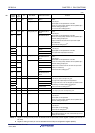
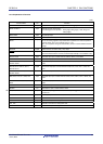
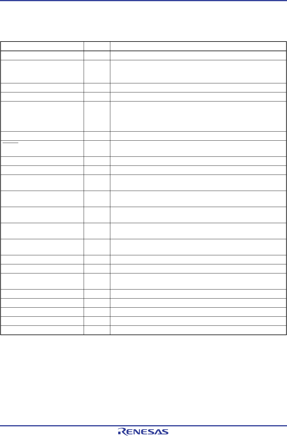
Function Name I/O Function
ANI0 to ANI12, ANI16 to ANI30 Input A/D converter analog input (see Figure 11-44 Analog Input Pin Connection)
INTP0 to INTP11 Input
External interrupt request input
The valid edge can be specified : Rising edge, falling edge, or both rising and
falling edges)
KR0 to KR9 Input Key interrupt input
PCLBUZ0, PCLBUZ1 Output Clock output/buzzer output
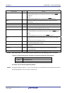
REGC
−
Pin for connecting regulator output stabilization capacitance for internal operation.
Connect this pin to V
SS via a capacitor (0.47 to 1
μ
F).
Also, use a capacitor with good characteristics, since it is used to stabilize internal
voltage.
RTC1HZ Output Real-time clock correction clock (1 Hz) output
RESET Input
This is the active-low system reset input pin.
When the external reset is not used, connect this pin directly or via a resistor to V
DD.
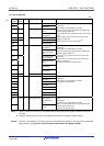
RxD0 to RxD2 Input Serial data input pins of serial interface UART0, UART1, and UART2
TxD0 to TxD2 Output Serial data output pins of serial interface UART0, UART1, and UART2
SCK00, SCK01, SCK10, SCK11,
SCK20, SCK21
I/O
Serial clock I/O pins of serial interface CSI00, CSI01, CSI10, CSI11, CSI20, and
CSI21
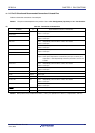
SCL00, SCL01, SCL10, SCL11,
SCL20, SCL21
Output
Serial clock output pins of serial interface IIC00, IIC01, IIC10, IIC11, IIC20, and
IIC21
SDA00, SDA01, SDA10, SDA11,
SDA20, SDA21
I/O
Serial data I/O pins of serial interface IIC00, IIC01, IIC10, IIC11, IIC20, and IIC21
SI00, SI01, SI10, SI11, SI20, SI21 Input
Serial data input pins of serial interface CSI00, CSI01, CSI10, CSI11, CSI20, and
CSI21
SO00, SO01, SO10, SO11, SO20,
SO21
Output
Serial data output pins of serial interface CSI00, CSI01, CSI10, CSI11, CSI20, and
CSI21
SCLA0 I/O Serial clock I/O pins of serial interface IICA0
SDAA0 I/O Serial data I/O pins of serial interface IICA0
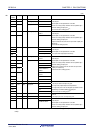
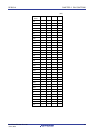
TI00, TI01, TI03 to TI07 Input
The pins for inputting an external count clock/capture trigger to 16-bit timers 00, 01,
and 03 to 07
TO00, TO01, TO03 to TO07 Output Timer output pins of 16-bit timers 00, 01, and 03 to 07
X1, X2
−
Resonator connection for main system clock
EXCLK Input External clock input for main system clock
XT1, XT2
−
Resonator connection for subsystem clock
EXCLKS Input External clock input for subsystem clock
<R>
R01UH0305EJ0200 Rev.2.00 33
Jul 04, 2013