


RL78/G1A CHAPTER 12 SERIAL ARRAY UNIT
R01UH0305EJ0200 Rev.2.00 429
Jul 04, 2013
12.3.15 Input switch control register (ISC)
The ISC1 and ISC0 bits of the ISC register are used to realize a LIN-bus communication operation by UART2 in
coordination with an external interrupt and the timer array unit.
When bit 0 is set to 1, the input signal of the serial data input (R
XD2) pin is selected as an external interrupt (INTP0)
that can be used to detect a wakeup signal.
When bit 1 is set to 1, the input signal of the serial data input (R
XD2) pin is selected as a timer input, so that wake up
signal can be detected, the low width of the break field, and the pulse width of the sync field can be measured by the timer.
The ISC register can be set by a 1-bit or 8-bit memory manipulation instruction.
Reset signal generation clears the ISC register to 00H.
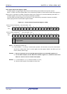
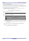
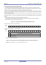
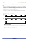
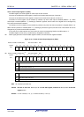
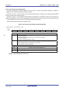
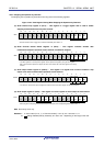
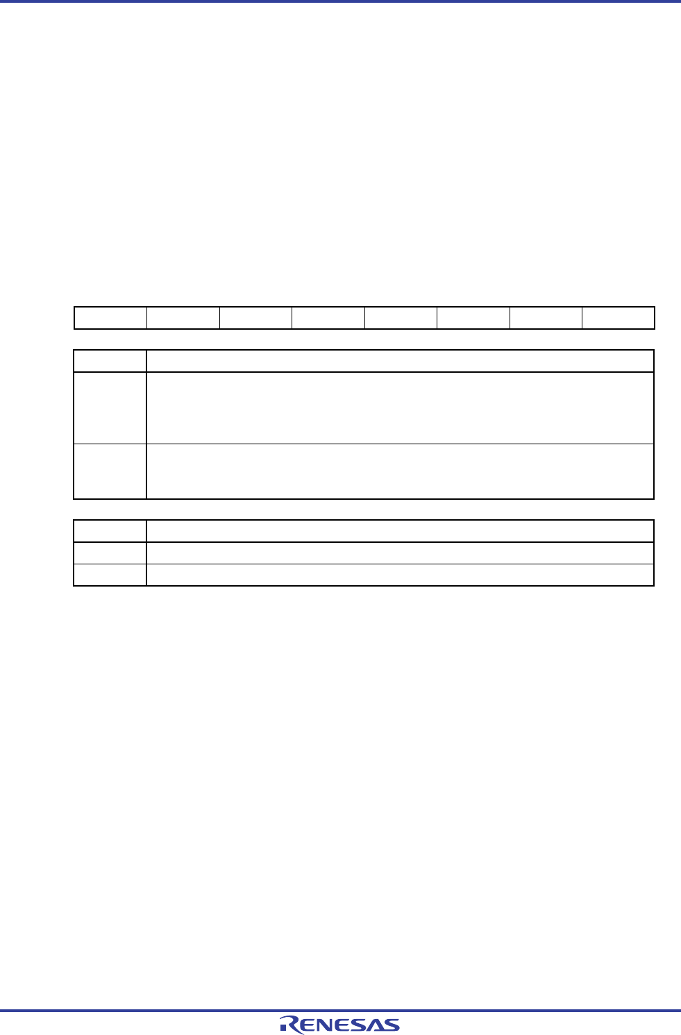
Figure 12-20. Format of Input Switch Control Register (ISC)
Address: F0073H After reset: 00H R/W
Symbol 7 6 5 4 3 2 1 0
ISC 0 0 0 0 0 0 ISC1 ISC0
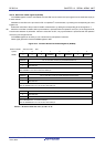
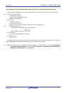
ISC1 Switching channel 7 input of timer array unit
0
48- and 64-pin products:
Uses the input signal of the TI07 pin as a timer input (normal operation).
25- and 32-pin products:
Do not use a timer input signal for channel 7.
1
Input signal of the R
XD2 pin is used as timer input (detects the wakeup signal and measures the low
width of the break field and the pulse width of the sync field).
Setting is prohibited in the 25-pin products.
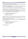
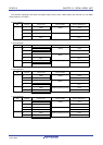
ISC0 Switching external interrupt (INTP0) input
0 Uses the input signal of the INTP0 pin as an external interrupt (normal operation).
1 Uses the input signal of the RXD2 pin as an external interrupt (wakeup signal detection).
Caution Be sure to clear bits 7 to 2 to “0”.
<R>