


RL78/G1A CHAPTER 11 A/D CONVERTER
R01UH0305EJ0200 Rev.2.00 388
Jul 04, 2013
11.7.4 Setup when temperature sensor output voltage/internal reference voltage is selected (example for software
trigger mode and one-shot conversion mode)
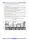
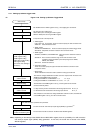
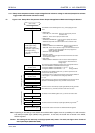
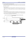
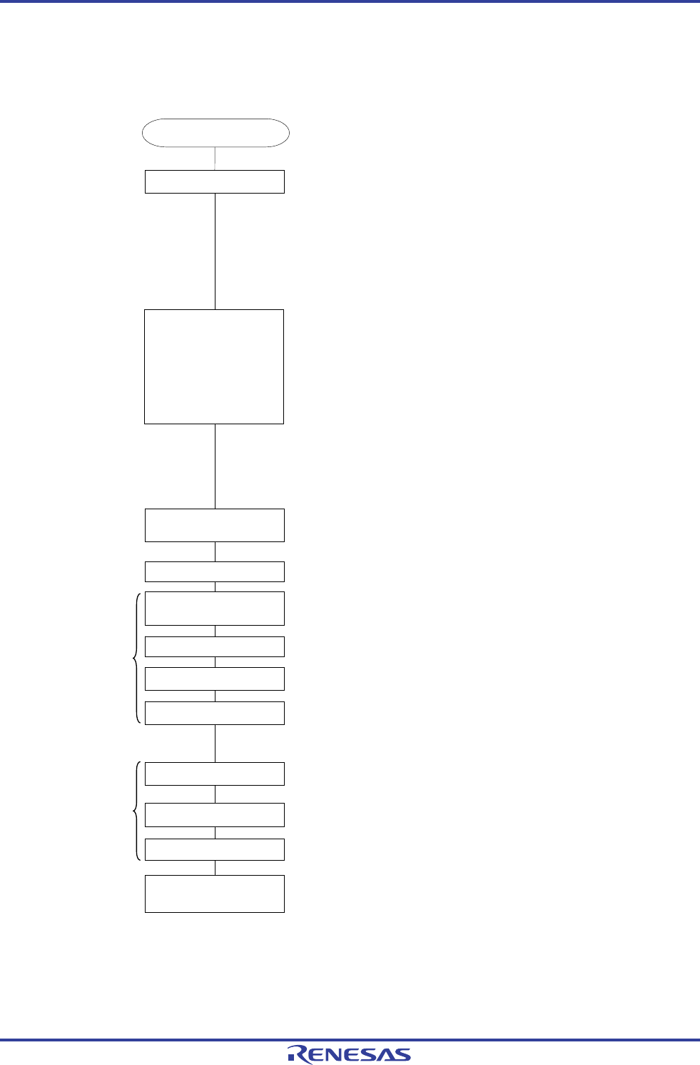
Figure 11-32. Setup When Temperature Sensor Output Voltage/Internal Reference Voltage Is Selected
PER0 register setting
The ADCEN bit of the PER0 register is set (1), and supplying the clock
starts.
• ADM0 register
FR2 to FR0, LV1, and LV0 bits: These are used to specify the A/D
conversion time.
ADMD bit: This is used to specify the select mode.
• ADM1 register
ADTMD1 and ADTMD0 bits: These are used to specify the software
trigger mode.
ADSCM bit: Sequential conversion mode/one-shot conversion mode
•
ADM2 register
ADREFP1, ADREFP0, and ADREFM bits: These are used to select the
reference voltage.
ADRCK bit: This is used to select the range for the A/D conversion result
comparison value generated by the interrupt signal from
AREA1, AREA3, and AREA2.
ADTYP bit: 8-bit/12-bit resolution
• ADUL/ADLL register
These are used to specify the upper limit and lower limit A/D conversion
result comparison values.
• ADS register
ADISS and ADS4 to ADS0 bits: These are used to select temperature
sensor 0 output or internal reference
voltage output.
The ADCE bit of the ADM0 register is set (1), and the system enters the
A/D conversion standby status.
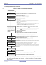
If a temperature sensor output/internal reference voltage output (ADISS bit
of ADS register = 1) are selected as the analog input channel:
B = 2
μ
s
The A/D conversion end interrupt request signal (INTAD) is generated.
Note
The conversion results are stored in the ADCR and ADCRH registers.
After completion of the reference voltage stabilization wait time count B, the
ADCS bit of the ADM0 register is set (1), and A/D conversion starts
Start of setup
The A/D conversion end interrupt request signal (INTAD) will be generated.
After ADISS is set (1), the initial conversion result cannot be used.
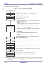
The ADCS bit of the ADM0 register is set (1), and A/D conversion starts.
First A/D conversion time
The reference voltage stabilization wait time count A is required when the
value of the ADREFP1 and ADREFP0 bits is changed.
If change the ADREFP1 and ADREFP0 = 0, 0 or 0, 1: A = 1
μ
s
If change the ADREFP1 and ADREFP0 = 1, 0: Setting prohibited
Second A/D conversion time
• ADM0 register setting
• ADM1 register setting
• ADM2 register setting
• ADUL/ADLL register setting
• ADS register setting
(The order of the settings is
irrelevant.)
ADCE bit setting
Reference voltage stabilization
wait time count B
Start of A/D conversion
End of A/D conversion
ADCS bit setting
Storage of conversion results in
the ADCR and ADCRH registers
End of A/D conversion
ADCS bit setting
Start of A/D conversion
Reference voltage stabilization
wait time count A
Note Depending on the settings of the ADRCK bit and ADUL/ADLL register, there is a possibility of no A/D conversion
end interrupt request signal (INTAD) being generated. In this case, the results are not stored in the ADCR,
ADCRH registers.
Caution This setting can be used only in HS (high-speed main) mode. For detail, see Figure 24-3 Format of
User Option Byte (000C2H/010C2H).
<R>