


RL78/G1A CHAPTER 11 A/D CONVERTER
R01UH0305EJ0200 Rev.2.00 357
Jul 04, 2013
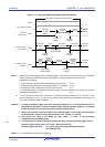
Notes 1. For the second and subsequent conversion in sequential conversion mode and for conversion of the channel
specified by scan 1, 2, and 3 in scan mode, the conversion start time and stabilization wait time for A/D power
supply do not occur after a hardware trigger is detected (see Table 11-3 (3/4)).
2. When using ANI16 to ANI30, setting this value is prohibited.
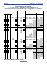
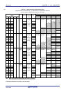
Cautions 1. The A/D conversion time must also be within the relevant range of conversion times (t
CONV)
described in 29.6.1 or 30.6.1 A/D converter characteristics.
2. When rewriting the FR2 to FR0, LV1, and LV0 bits to other than the same data, while in the
conversion stopped (ADCS = 0, ADCE = 0).
3. The above conversion time does not include clock frequency errors. Select conversion time, taking
clock frequency errors into consideration.
4. When hardware trigger wait mode, specify the conversion time so that the following conditions are
satisfied:
• f
AD is used within a range of 1 to 16 MHz.
• When using ANI16 to ANI30, the A/D converter is used in the following conditions:
When LV1 = 0, LV0 = 0: Setting prohibit
When LV1 = 0, LV0 = 1: 2.4 V ≤ AVDD ≤ 3.6 V
When LV1 = 1, LV0 = 0: 1.8 V ≤ AVDD ≤ 3.6 V, 1 MHz ≤ fCLK ≤ 8 MHz
When LV1 = 1, LV0 = 1: 1.6 V ≤ AVDD ≤ 3.6 V, 1 MHz ≤ fCLK ≤ 4 MHz
• Condition when temperature sensor or internal reference voltage (ADISS bit of ADS register = 1)
is set for the analog input channel:
When LV1 = 0, LV0 = 0: Setting prohibit
When LV1 = 0, LV0 = 1: 2.4 V ≤ AV
DD ≤ 3.6 V
When LV1 = 1, LV0 = 0: 2.4 V ≤ AV
DD ≤ 3.6 V, 1 MHz ≤ fCLK ≤ 8 MHz
When LV1 = 1, LV0 = 1: 2.4 V ≤ AV
DD ≤ 3.6 V, 1 MHz ≤ fCLK ≤ 4 MHz
Remark f
CLK: CPU/peripheral hardware clock frequency