


RL78/G1A CHAPTER 11 A/D CONVERTER
R01UH0305EJ0200 Rev.2.00 396
Jul 04, 2013
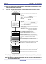
11.10 Cautions for A/D Converter
(1) Operating current in STOP mode
Shift to STOP mode after stopping the A/D converter (by setting bit 7 (ADCS) of A/D converter mode register 0
(ADM0) to 0). The operating current can be reduced by setting bit 0 (ADCE) of the ADM0 register to 0 at the same
time.
To restart from the standby status, clear bit 0 (ADIF) of interrupt request flag register 1H (IF1H) to 0 and start
operation.
(2) Input range of ANI0 to ANI12 and ANI16 to ANI30 pins
Observe the rated range of the ANI0 to ANI12 and ANI16 to ANI30 pins input voltage. If a voltage of AV
DD, and
AV
REFP or higher and AVSS, and AVREFM or lower (even in the range of absolute maximum ratings) is input to an
analog input channel, the converted value of that channel becomes undefined. In addition, the converted values of
the other channels may also be affected.
When internal reference voltage (1.45 V) is selected reference voltage for the + side of the A/D converter, do not input
internal reference voltage (1.45 V) or higher voltage to a pin selected by the ADS register. However, it is no problem
that a pin not selected by the ADS register is input voltage greater than the internal reference voltage (1.45 V).
Caution Internal reference voltage (1.45 V) can be used only in HS (high-speed main) mode. For detail, see
Figure 24-3 Format of User Option Byte (000C2H/010C2H).
(3) Conflicting operations
<1> Conflict between the A/D conversion result register (ADCR, ADCRH) write and the ADCR or ADCRH register
read by instruction upon the end of conversion
The ADCR or ADCRH register read has priority. After the read operation, the new conversion result is written to
the ADCR or ADCRH registers.
<2> Conflict between the ADCR or ADCRH register write and the A/D converter mode register 0 (ADM0) write, the
analog input channel specification register (ADS), or A/D port configuration register (ADPC) write upon the end
of conversion
The ADM0, ADS, or ADPC registers write has priority. The ADCR or ADCRH register write is not performed,
nor is the conversion end interrupt request signal (INTAD) generated.
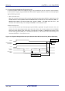
(4) Noise countermeasures
To maintain the 12-bit resolution, attention must be paid to noise input to the AV
REFP, AVDD, ANI0 to ANI12, and ANI16
to ANI30 pins.
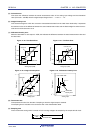
<1> Connect a capacitor with a low equivalent resistance and a good frequency response (capacitance of about
0.01
μ
F) via the shortest possible run of relatively thick wiring to the power supply.
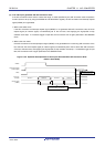
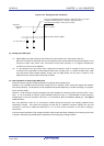
<2> The higher the output impedance of the analog input source, the greater the influence. To reduce the noise,
connecting external capacitor as shown in Figure 11-44 is recommended.
<3> Do not switch these pins with other pins during conversion.
<4> The accuracy is improved if the HALT mode is set immediately after the start of conversion.
<5> Separate digital and analog signals so that they do not cross or approach each other.
<R>