


RL78/G1A CHAPTER 11 A/D CONVERTER
R01UH0305EJ0200 Rev.2.00 365
Jul 04, 2013
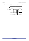
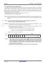
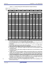
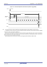
Figure 11-11. Format of Analog Input Channel Specification Register (ADS) (2/2)
Address: FFF31H After reset: 00H R/W
Symbol 7 6 5 4 3 2 1 0
ADS ADISS 0 0 ADS4 ADS3 ADS2 ADS1 ADS0
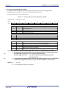
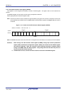
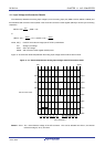
{ Scan mode (ADMD = 1)
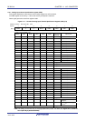
Analog input channel ADISS ADS4 ADS3 ADS2 ADS1 ADS0
Scan 0 Scan 1 Scan 2 Scan 3
0 0 0 0 0 0 ANI0 ANI1 ANI2 ANI3
0 0 0 0 0 1 ANI1 ANI2 ANI3 ANI4
0 0 0 0 1 0 ANI2 ANI3 ANI4 ANI5
0 0 0 0 1 1 ANI3 ANI4 ANI5 ANI6
0 0 0 1 0 0 ANI4 ANI5 ANI6 ANI7
0 0 0 1 0 1 ANI5 ANI6 ANI7 ANI8
0 0 0 1 1 0 ANI6 ANI7 ANI8 ANI9
0 0 0 1 1 1 ANI7 ANI8 ANI9 ANI10
0 0 1 0 0 0 ANI8 ANI9 ANI10 ANI11
0 0 1 0 0 1 ANI9 ANI10 ANI11 ANI12
0 1 0 0 0 0 ANI16 ANI17 ANI18 ANI19
0 1 0 0 0 1 ANI17 ANI18 ANI19 ANI20
0 1 0 0 1 0 ANI18 ANI19 ANI20 ANI21
0 1 0 0 1 1 ANI19 ANI20 ANI21 ANI22
0 1 0 1 0 0 ANI20 ANI21 ANI22 ANI23
0 1 0 1 0 1 ANI21 ANI22 ANI23 ANI24
0 1 0 1 1 0 ANI22 ANI23 ANI24 ANI25
0 1 0 1 1 1 ANI23 ANI24 ANI25 ANI26
0 1 1 0 0 0 ANI24 ANI25 ANI26 ANI27
0 1 1 0 0 1 ANI25 ANI26 ANI27 ANI28
0 1 1 0 1 0 ANI26 ANI27 ANI28 ANI29
0 1 1 0 1 1 ANI27 ANI28 ANI29 ANI30
Other than above Setting prohibited
Cautions 1. Be sure to clear bits 5 and 6 to 0.
2 Set a channel to be set the analog input by ADPC and PMCx registers in the input mode by using
port mode registers0 to 5, 7, 12, or 15 (PM0 to PM5, PM7, PM12, PM15).
3. Do not set the pin that is set by the A/D port configuration register (ADPC) as digital I/O by the
ADS register.
4. Do not set the pin that is set by port mode control register 0, 1, 3 to 5, 7, or 12 (PMC0, PMC1,
PMC3 to PMC5, PMC7, PMC12) as digital I/O by the ADS register.
5. Rewrite the value of the ADISS bit while conversion operation is stopped (ADCS = 0, ADCE = 0).
6. If using AV
REFP as the + side reference voltage of the A/D converter, do not select ANI0 as an A/D
conversion channel.
7. If using AV
REFM as the − side reference voltage of the A/D converter, do not select ANI1 as an A/D
conversion channel.
8. If ADISS is set to 1, the internal reference voltage (1.45 V) cannot be used for the + side reference
voltage. Also, after setting the ADISS to 1, the result of the first conversion cannot be used. For
details about the setting flow, see 11.7.4 Setup when temperature sensor output voltage/internal
reference voltage is selected (example for software trigger mode and one-shot conversion mode).
9. Do not set the ADISS bit to 1 when shifting to STOP mode, or to HALT mode while the CPU is
operating on the subsystem clock. When the ADISS bit is set to 1, the current value of the
temperature sensor operating current (I
TMPS) and A/D converter reference voltage current (IADREF)
indicated in 29.3.2 or 30.3.2 Supply current characteristics will be added.
10. Ignore the conversion result if the corresponding ANI pin does not exist depending on the
product (number of pins).
<R>