


RL78/G1A CHAPTER 11 A/D CONVERTER
R01UH0305EJ0200 Rev.2.00 369
Jul 04, 2013
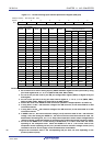
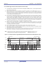
11.4 A/D Converter Conversion Operations
The A/D converter conversion operations are described below.
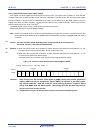
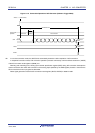
<1> The voltage input to the selected analog input channel is sampled by the sample & hold circuit.
<2> When sampling has been done for a certain time, the sample & hold circuit is placed in the hold state and the
sampled voltage is held until the A/D conversion operation has ended.
<3> Bit 11 of the successive approximation register (SAR) is set. The series resistor string voltage tap is set to (1/2)
AV
REF by the tap selector.
<4> The voltage difference between the series resistor string voltage tap and sampled voltage is compared by the
voltage comparator. If the analog input is greater than (1/2) AV
REF, the MSB bit of the SAR register remains set
to 1. If the analog input is smaller than (1/2) AV
REF, the MSB bit is reset to 0.
<5> Next, bit 10 of the SAR register is automatically set to 1, and the operation proceeds to the next comparison. The
series resistor string voltage tap is selected according to the preset value of bit 11, as described below.
• Bit 11 = 1: (3/4) AV
REF
• Bit 11 = 0: (1/4) AV
REF
The voltage tap and sampled voltage are compared and bit 10 of the SAR register is manipulated as follows.
• Sampled voltage ≥ Voltage tap: Bit 10 = 1
• Sampled voltage < Voltage tap: Bit 10 = 0
<6> Comparison is continued in this way up to bit 0 of the SAR register.
<7> Upon completion of the comparison of 12 bits, an effective digital result value remains in the SAR register, and
the result value is transferred to the A/D conversion result register (ADCR, ADCRH) and then latched
Note 1
.
At the same time, the A/D conversion end interrupt request signal (INTAD) can also be generated
Note 1
.
<8> Repeat steps <1> to <7>, until the ADCS bit is cleared to 0
Note 2
.
To stop the A/D converter, clear the ADCS bit to 0.
Notes 1. If the A/D conversion result is outside the A/D conversion result range specified by the ADRCK bit and the
ADUL and ADLL registers (see Figure 11-8), the A/D conversion result interrupt request signal is not
generated and no A/D conversion results are stored in the ADCR and ADCRH registers.
2. While in the sequential conversion mode, the ADCS flag is not automatically cleared to 0. This flag is not
automatically cleared to 0 while in the one-shot conversion mode of the hardware trigger no-wait mode,
either. Instead, 1 is retained.
Remarks 1. Two types of the A/D conversion result registers are available.
• ADCR register (16 bits): Store 12-bit A/D conversion value
• ADCRH register (8 bits): Store 8-bit A/D conversion value
2. AV
REF: The + side reference voltage of the A/D converter. This can be selected from AVREFP, the
internal reference voltage (1.45 V), and AV
DD.