


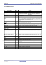
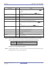
RL78/G1A CHAPTER 2 PIN FUNCTIONS
(2/2)
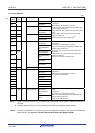
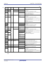
Function Name I/O Function
VDD
−
<25-pin, 32-pin 48-pin>
Positive power supply for port pin other than P20 to P27, P150 and RESET,
REGC pin.
<64-pin >
Positive power supply for P121 to P124, P137 and RESET, REGC pin.
EVDD0
−
Positive power supply for ports (other than P20 to P27, P121 to P124, P137,
P150 to P154)
AVDD
−
Positive power supply for P20 to P27, P150 to P154, and A/D converter
AVREFP Input A/D converter reference potential (+ side) input
AVREFM Input
A/D converter reference potential (− side) input
Make AV
REFM pin the same potential as AVSS and VSS pin.
VSS
−
<25-pin, 32-pin, 48-pin>
Ground potential for port pin other than P20 to P27, P150 and RESET, REGC
pin.
<64-pin>
Ground potential for P121 to P124, P137 and RESET, REGC pin.
EVSS0
−
Ground potential for ports (other than P20 to P27, P121 to P124, P137, P150 to
P154)
Make EV
SS0 pin the same potential as VSS pin.
AVSS
−
Ground potential for A/D converter, P20 to P27, and P150 to P154. Use this pin
with the same potential as EV
SS0, and VSS.
TOOLRxD Input
UART reception pin for the external device connection used during flash memory
programming
TOOLTxD Output
UART transmission pin for the external device connection used during flash
memory programming
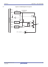
TOOL0 I/O Data I/O for flash memory programmer/debugger
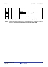
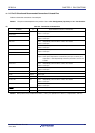
Caution After reset release, the relationships between P40/TOOL0 and the operating mode are as follows.
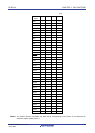
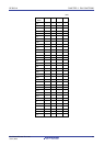
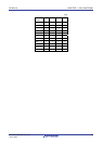
Table 2-2. Relationships Between P40/TOOL0 and Operation Mode After Reset Release
P40/TOOL0 Operating Mode
EVDD0 Normal operation mode
0 V Flash memory programming mode
For details, see 25.4 Serial Programming Method.
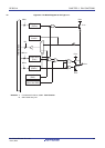
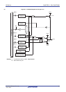
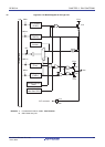
Remark Use bypass capacitors (about 0.1
μ
F) as noise and latch up countermeasures with relatively thick wires at
the shortest distance to V
DD to VSS, EVDD0 to EVSS0 lines.
R01UH0305EJ0200 Rev.2.00 34
Jul 04, 2013