


RL78/G1A CHAPTER 29 ELECTRICAL SPECIFICATIONS (T
A = −40 to +85°C)
R01UH0305EJ0200 Rev.2.00 872
Jul 04, 2013
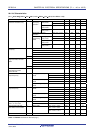
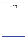
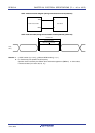
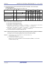
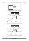
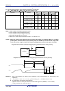
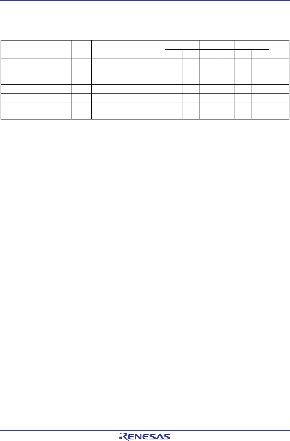
(2) During communication at same potential (CSI mode) (master mode, SCKp... internal clock output,
corresponding CSI00 only)
(T
A = −40 to +85°C, 2.7 V ≤ EVDD0 ≤ VDD ≤ 3.6 V, VSS = EVSS0 = 0 V)
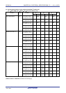
Notes 1. HS is condition of HS (high-speed main) mode.
2. LS is condition of LS (low-speed main) mode.
3. LV is condition of LV (low-voltage main) mode.
4. When DAPmn = 0 and CKPmn = 0, or DAPmn = 1 and CKPmn = 1. The SIp setup time or SIp hold time
becomes “from SCKp↓” when DAPmn = 0 and CKPmn = 1, or DAPmn = 1 and CKPmn = 0.
5. When DAPmn = 0 and CKPmn = 0, or DAPmn = 1 and CKPmn = 1. The delay time to SOp output becomes
“from SCKp↑” when DAPmn = 0 and CKPmn = 1, or DAPmn = 1 and CKPmn = 0.
6. C is the load capacitance of the SCKp and SOp output lines.
Caution Select the normal input buffer for the SIp pin and the normal output mode for the SOp pin and SCKp pin
by using port input mode register g (PIMg) and port output mode register g (POMg).
Remarks 1. p: CSI number (p = 00), m: Unit number (m = 0), n: Channel number (n = 0),
g: PIM and POM numbers (g = 1)
2. f
MCK: Serial array unit operation clock frequency
(Operation clock to be set by the CKSmn bit of serial mode register mn (SMRmn). m: Unit number,
n: Channel number (mn = 00))
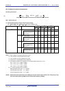
HS
Note 1
LS
Note 2
LV
Note 3
Parameter Symbol Conditions
MIN. MAX. MIN. MAX. MIN. MAX.
Unit
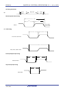
SCKp cycle time tKCY1 2.7 V ≤ EVDD ≤ 3.6 V tKCY1 ≥ 2/fCLK 83.3 250 500 ns
SCKp high-/low-level width
t
KH1,
t
KL1
2.7 V ≤ EV
DD ≤ 3.6 V
t
KCY1/2
−10
tKCY1/2
−50
tKCY1/2
−50
ns
SIp setup time (to SCKp↑)
Note 4
tSIK1 2.7 V ≤ EVDD ≤ 3.6 V 33 110 110 ns
SIp hold time (from SCKp↑)
Note 4
tKSI1 2.7 V ≤ EVDD ≤ 3.6 V 10 10 10 ns
Delay time from SCKp↓ to
SOp output
Note 5
t
KSO1 C = 20 pF
Note 6
10 10 10 ns