


R01UH0305EJ0200
Rev.2.00
Jul 04, 2013
RL78/G1A
RENESAS MCU
CHAPTER 1 OUTLINE
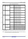
1.1 Features
<R>
Ultra-low power consumption technology
• V
DD = single power supply voltage of 1.6 to 3.6 V which can operate a 1.8 V device at a low voltage
• HALT mode
• STOP mode
• SNOOZE mode
RL78 CPU core
• CISC architecture with 3-stage pipeline
• Minimum instruction execution time: Can be changed from high speed (0.03125 μs: @ 32 MHz operation with high-
speed on-chip oscillator) to ultra-low speed (30.5 μs: @ 32.768 kHz operation with subsystem clock)
• Address space: 1 MB
• General-purpose registers: (8-bit register × 8) × 4 banks
• On-chip RAM: 2 to 4 KB
Code flash memory
• Code flash memory: 16 to 64 KB
• Block size: 1 KB
• Prohibition of block erase and rewriting (security function)
• On-chip debug function
• Self-programming (with boot swap function/flash shield window function)
Data flash memory
• Data flash memory: 4 KB
• Back ground operation (BGO): Instructions can be executed from the program memory while rewriting the data flash
memory.
• Number of rewrites: 1,000,000 times (TYP.)
• Voltage of rewrites: V
DD = 1.8 to 3.6 V
High-speed on-chip oscillator
• Select from 32 MHz, 24 MHz, 16 MHz, 12 MHz, 8 MHz, 6 MHz, 4 MHz, 3 MHz, 2 MHz, and 1 MHz
• High accuracy ±1.0 % (V
DD = 1.8 to 3.6 V, TA = -20 to +85°C)
Operating ambient temperature
• T
A = -40 to +85°C (A: Consumer applications)
• T
A = -40 to +105°C (G: Industrial applications)
Power management and reset function
• On-chip power-on-reset (POR) circuit
• On-chip voltage detector (LVD) (Select interrupt and reset from 12 levels)
R01UH0305EJ0200 Rev.2.00 1
Jul 04, 2013