


RL78/G1A CHAPTER 20 POWER-ON-RESET CIRCUIT
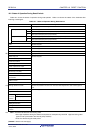
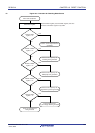
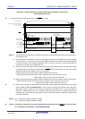
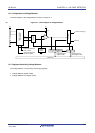
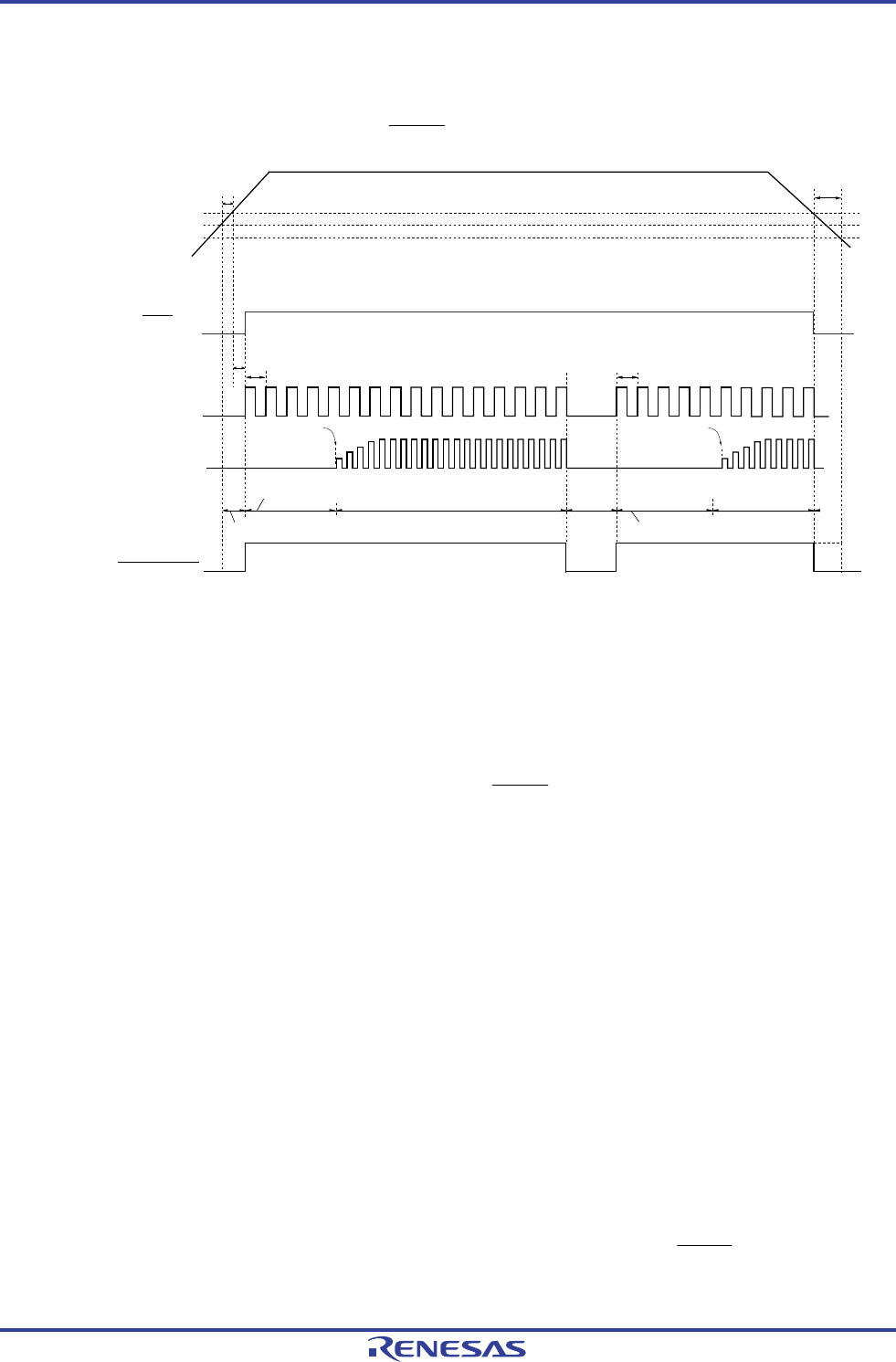
Figure 20-2. Timing of Generation of Internal Reset Signal by Power-on-reset Circuit
and Voltage Detector (1/3)
(1) When the externally input reset signal on the RESET pin is used
<R>
Jul 04, 2013
Note 5
Note 5
Supply voltage (V
DD
)
Lower limit voltage for guaranteed operation
V
POR
= 1.51 V (TYP.)
V
PDR
= 1.50 V (TYP.)
0 V
RESET pin
High-speed on-chip
oscillator clock (f
IH
)
High-speedsystem
clock (f
MX
)
(when X1 oscillation
is selected)
CPU Operation stops
Internal reset signal
Starting oscillation
is specified
by software
At least 10 μs
Reset
period
(oscillation
stop)
Starting oscillation
is specified by software
Reset processing time when
external reset is released.
Normal operation
(high-speed on-chip
oscillator clock)
Normal operation (high-speed
on-chip oscillator clock)
Operation stops
Wait for oscillation
accuracy stabilization
Wait for oscillation
accuracy stabilization
Note 2
Note 4
Note 3
Note 2
Reset processing time
when external reset
is released.
Note 1
Note 1
Voltage stabilization wait
0.99 ms (TYP.), 2.30 ms (MAX.)
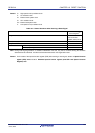
Notes 1. The internal reset processing time includes the oscillation accuracy stabilization time of the high-speed on-
chip oscillator clock.
2. The high-speed on-chip oscillator clock and a high-speed system clock or subsystem clock can be selected
as the CPU clock. To use the X1 clock, use the oscillation stabilization time counter status register (OSTC)
to confirm the lapse of the oscillation stabilization time. To use the XT1 clock, use the timer function for
confirmation of the lapse of the stabilization time.
3. The time until normal operation starts includes the following reset processing time when the external reset
is released (after the first release of POR) after the RESET signal is driven high (1) as well as the voltage
stabilization wait time after VPOR (1.51 V, typ.) is reached.
Reset processing time when the external reset is released is shown below.
After the first release of POR: 0.672 ms (typ.), 0.832 ms (max.) (when the LVD is in use)
0.399 ms (typ.), 0.519 ms (max.) (when the LVD is off)
4. Reset processing time when the external reset is released after the second release of POR is shown below.
After the second release of POR: 0.531 ms (typ.), 0.675 ms (max.) (when the LVD is in use)
0.259 ms (typ.), 0.362 ms (max.) (when the LVD is off)
5. After power is supplied, the reset state must be retained until the operating voltage becomes in the range
defined in 29.4 or 30.4 AC Characteristics. This is done by controlling the externally input reset signal.
After power supply is turned off, this LSI should be placed in the STOP mode, or in the reset state by
utilizing the voltage detection circuit or externally input reset signal, before the voltage falls below the
operating range. When restarting the operation, make sure that the operation voltage has returned within
the range of operation.
Remark V
POR: POR power supply rise detection voltage
VPDR: POR power supply fall detection voltage
<R>
<R>
Caution For power-on reset, be sure to use the externally input reset signal on the RESET pin when the LVD is
off. For details, see CHAPTER 21 VOLTAGE DETECTOR.
R01UH0305EJ0200 Rev.2.00 751