


RL78/G1A APPENDIX A REVISION HISTORY
(4/11)
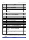
Page Description Classification
p.306 Modification of 7.3.10 Month count register (MONTH) (c)
p.309 Modification of 7.3.16 Port mode register 3 (PM3) (c)
p.309 Modification of 7.3.17 Port register 3 (P3) (c)
p.315 Modification of 7.4.5 1 Hz output of real-time clock (c)
p.317
Modification of Correction example 1 in 7.4.6 Example of watch error correction of real-
time clock
(c)
p.318
Modification of Figure 7-25. Correction Operation when (DEV, F6, F5, F4, F3, F2, F1, F0) =
(0, 0, 1, 0, 1, 1, 0, 0)
(c)
p.320
Modification of Figure 7-26. Correction Operation when (DEV, F6, F5, F4, F3, F2, F1, F0) =
(1, 1, 1, 0, 1, 1, 1, 0)
(c)
CHAPTER 8 12-BIT INTERVAL TIMER
p.321 Modification of 8.2 Configuration of 12-bit Interval Timer (c)
p.322 Modification of 8.3.1 Peripheral enable register 0 (PER0) (c)
p.325 Modification of Figure 8-5. 12-bit Interval Timer Operation Timing (c)
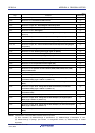
CHAPTER 9 CLOCK OUTPUT/BUZZER OUTPUT CONTROLLER
p.327 Modification of 9.1 Functions of Clock Output/Buzzer Output Controller (c)
p.330 Modification of Figure 9-2. Format of Clock Output Select Register n (CKSn) (c)
p.331
Modification of 9.3.2 Registers controlling port functions of pins to be used for clock or
buzzer output
(c)
p.332 Modification of 9.4 Operations of Clock Output/Buzzer Output Controller (c)
CHAPTER 10 WATCHDOG TIMER
p.333 Modification of 10.1 Functions of Watchdog Timer (c)
p.334 Modification of 10.2 Configuration of Watchdog Timer (c)
p.336 Modification of 10.4.1 Controlling operation of watchdog timer (c)
p.337 Modification of Table 10-3. Setting of Overflow Time of Watchdog Timer (c)
CHAPTER 11 A/D CONVERTER
p.340, 341 Modification of 11.1 Function of A/D Converter (c)
p.346 Modification of Figure 11-2. Format of Peripheral Enable Register 0 (PER0) (c)
p.347 Modification of Figure 11-3. Format of A/D Converter Mode Register 0 (ADM0) (c)
p.350 to 357 Modification of Table 11-3. A/D Conversion Time Selection (c)
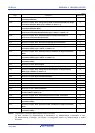
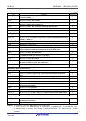
p.359 Modification of Figure 11-6. Format of A/D Converter Mode Register 1 (ADM1) (c)
p.361 Modification of Figure 11-7. Format of A/D Converter Mode Register 2 (ADM2) (2/2) (c)
p.362 Modification of 11.3.5 12-bit A/D conversion result register (ADCR) (c)
p.365
Modification of Figure 11-11. Format of Analog Input Channel Specification Register
(ADS) (2/2)
(c)
p.367 Modification of 11.3.10 A/D test register (ADTES) and addition of Caution (c)
p.368 Modification of 11.3.11 Registers controlling port function of analog input pins (c)
p.370
Modification of Figure 11-15. Conversion Operation of A/D Converter (Software Trigger
Mode)
(c)
p.385 to 389, 393 Modification of Figures 11-29, 11-30, 11-31, 11-32, 11-33, and 11-37 (c)
p.389 Modification of Figure 11-33. Setting up Test Mode (c)
Remark “Classification” in the above table classifies revisions as follows.
(a): Error correction, (b): Addition/change of specifications, (c): Addition/change of description or note,
(d): Addition/change of package, part number, or management division, (e): Addition/change of related
documents
R01UH0305EJ0200 Rev.2.00 961
Jul 04, 2013