


RL78/G1A CHAPTER 11 A/D CONVERTER
R01UH0305EJ0200 Rev.2.00 360
Jul 04, 2013
11.3.4 A/D converter mode register 2 (ADM2)
This register is used to select the + side or - side reference voltage of the A/D converter, check the upper limit and
lower limit A/D conversion result values, select the resolution, and specify whether to use the SNOOZE mode.
The ADM2 register can be set by a 1-bit or 8-bit memory manipulation instruction.
Reset signal generation clears this register to 00H.
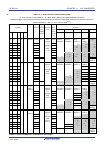
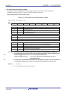
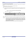
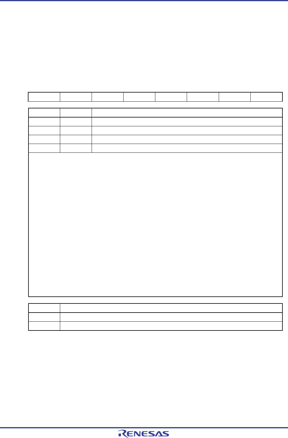
Figure 11-7. Format of A/D Converter Mode Register 2 (ADM2) (1/2)
Address: F0010H After reset: 00H R/W
Symbol 7 6 5 4 <3> <2> 1 <0>
ADM2 ADREFP1 ADREFP0 ADREFM 0 ADRCK AWC 0 ADTYP
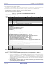
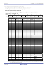
ADREFP1 ADREFP0 Selection of the + side reference voltage of the A/D converter
0 0 Supplied from AVDD
0 1 Supplied from P20/AVREFP/ANI0
1 0 Supplied from the internal reference voltage (1.45 V)
Note
1 1 Setting prohibited
• When ADREFP1 or ADREFP0 bit is rewritten, this must be configured in accordance with the following procedures.
(1) Set ADCE = 0
(2) Change the values of ADREFP1 and ADREFP0
(3) Reference voltage stabilization wait time (A)
(4) Set ADCE = 1
(5) Reference voltage stabilization wait time (B)
The stabilization wait time indicated by (3) is required when the value of the ADREFP1 and ADREFP0 bits is
changed.
When ADREFP1 and ADREFP0 are changed to 1 and 0: A = 10
μ
s
When ADREFP1 and ADREFP0 are changed to 0 and 0 or 0 and 1: A = 1
μ
s
The stabilization wait time indicated by (5) is required when the value of the ADCE bit is changed to 1.
If a high-accuracy channel is selected as the analog input channel: B = 0.5
μ
s
If a test mode setting (ADTES1 bit of ADTES register = 1) is selected: B = 0.5
μ
s
If a standard channel is selected as the analog input channel: B = 2
μ
s
If a temperature sensor/internal reference voltage are selected as the analog input channel: (ADISS bit of ADS
register = 1): B = 2
μ
s
After (5) stabilization time, start the A/D conversion.
• When ADREFP1 and ADREFP0 are set to 1 and 0, respectively, A/D conversion cannot be performed on the
temperature sensor output voltage and internal reference voltage (1.45 V).
Be sure to perform A/D conversion while ADISS = 0.
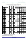
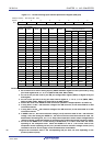
ADREFM Selection of the − side reference voltage of the A/D converter
0 Supplied from AVSS
1 Supplied from P21/AVREFM/ANI1
Note This setting can be used only in HS (high-speed main) mode. For detail, see Figure 24-3 Format of User
Option Byte (000C2H/010C2H).
Cautions 1. Rewrite the value of the ADM2 register while conversion is stopped (ADCS = 0, ADCE = 0).
2. Do not set the ADREFP1 bit to 1 when shifting to STOP mode, or to HALT mode while the CPU is
operating on the subsystem clock. Also, if the ADREFP1 bit is set to 1, the A/D converter
reference voltage current (I
ADREF) indicated in 29.3.2 or 30.3.2 Supply current characteristics will
be added to the current consumption when shifting to HALT mode while the CPU is operating on
the main system clock.
3. When using AV
REFP and AVREFM, specify ANI0 and ANI1 as the analog input channels and specify
input mode by using the port mode register.