


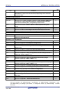
RL78/G1A APPENDIX A REVISION HISTORY
(1/8)
Edition Description Chapter
Renamed interval timer (unit) to 12-bit interval timer
Renamed VLVI, VLVIH, VLVIL to VLVD, VLVDH, VLVDL (LVD detection voltage)
Renamed interrupt source of RAM parity error (RAMTOP) to RPE
Though out
Modification of 1.2 Ordering Information
Addition of Figure 1-1. Part Number, Memory Size, and Package of RL78/G1A
Modification of 1.5.1 25-pin products to 1.5.4 64-pin products
CHAPTER 1 OUTLINE
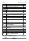
Modification of Table 2-1. Pin I/O Buffer Power Supplies
Modification of 2.1 Port Function
Modification of description in 2.2 Functions other than port pins (Deletion of
Description of Port Function)
Addition of remark to 2.3 Pin I/O Circuits and Recommended Connection of Unused
Pins
Change of Table 2-3. Connection of Unused Pins (64-pin products) (2/2)
CHAPTER 2 PIN
FUNCTIONS
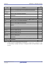
Addition of note 1 to Figures 3-1, 3-2
Addition of caution to Figures 3-1 to 3-4
Modification of note in Figures 3-3, 3-4
Addition of remark to Table 3-1. Correspondence Between Address Values and
Block Numbers in Flash Memory
Modification of caution 2 in 3.1.3 Internal data memory space
Addition of note 1 to Figures 3-6, 3-7
Addition of caution to Figures 3-6 to 3-9
Addition of note 1 to Figures 3-8, 3-9
Modification of caution 3 in 3.2.1 (3) Stack pointer (SP)
Deletion of caution 2 in 3.2.2 General-purpose registers
CHAPTER 3 CPU
ARCHITECTURE
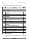
Modification of 4.1 Port Functions
Modification of block diagrams
Addition of description to 4.2.3 Port 2
Addition of description to 4.2.12 Port 15
Addition of caution to 4.3 Registers Controlling Port Function
Modification of Figure 4-39. Format of Port Register (64-pin products)
Modification of description and addition of caution to 4.3.3 Pull-up resistor option
registers (PUxx)
Addition of 4.3.5 Port output mode registers (POMxx)
Addition of cautions 1 and 2 to Figure 4-43. Format of Port Mode Control Register
Addition of caution 1 to Figure 4-44. Format of A/D Port Configuration Register
(ADPC)
Rev.0.03
Modification of description in 4.3.8 Peripheral I/O redirection register (PIOR)
CHAPTER 4 PORT
FUNCTIONS
R01UH0305EJ0200 Rev.2.00 974
Jul 04, 2013