


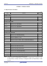
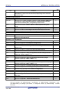
RL78/G1A APPENDIX A REVISION HISTORY
(9/11)
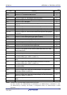
Page Description Classification
p.739
Modification of Figure 18-5. When the Interrupt Request Signal is Generated in the
SNOOZE Mod and Figure 18-6. When the Interrupt Request Signal is not Generated in
the SNOOZE Mode
(c)
CHAPTER 19 RESET FUNCTION
p.740 Modification of CHAPTER 19 RESET FUNCTION (c)
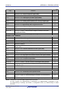
p.742, 743
Modification of figure, Note, and Caution in Figure 19-2. Timing of Reset by RESET Input
and Figure 19-3. Timing of Reset Due to Execution of Illegal Instruction, Watchdog
Timer Overflow, RAM Parity Error, or Illegal Memory Access Overflow
(c)
p.744
Modification of description and Note in Table 19-1. States of Operation During Reset
Period
(c)
p.746 Modification of Figure 19-4. Format of Reset Control Flag Register (RESF) (c)
p.747 Modification of Table 19-3. RESF Register Status When Reset Request Is Generated (c)
p.748 Modification of Figure 19-5. Procedure for Checking Reset Source (c)
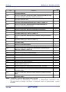
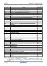
CHAPTER 20 POWER-ON-RESET CIRCUIT
p.749 Modification of 20.1 Functions of Power-on-reset Circuit (c)
p.751 to 753
Modification of Figure 20-2. Timing of Generation of Internal Reset Signal by Power-on-
reset Circuit and Voltage Detector
(c)
CHAPTER 21 VOLTAGE DETECTOR
p.754 Modification of 21.1 Functions of Voltage Detector (c)
p.755 Modification of Figure 21-1. Block Diagram of Voltage Detector (c)
p.756 Modification of Figure 21-2. Format of Voltage Detection Register (LVIM) (c)
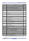
p.757
Modification of Note and Caution in Figure 21-3. Format of Voltage Detection Level Select
Register (LVIS)
(c)
p.758, 759 Modification of Table 21-1. Format of User Option Byte (000C1H/010C1H) (c)
p.760 Modification of 21.4.1 When used as reset mode (c)
p.761
Modification of Figure 21-4. Timing of Voltage Detector Internal Reset Signal Generation
(Option Byte LVIMDS1, LVIMDS0 = 1, 1)
(c)
p.762 Modification of 21.4.2 When used as interrupt mode (c)
p.763
Modification of Figure 21-5. Timing of Voltage Detector Internal Interrupt Signal
Generation (Option Byte LVIMDS1, LVIMDS0 = 0, 1)
(c)
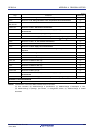
p.764 Modification of 21.4.3 When used as interrupt & reset mode (c)
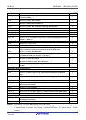
p.765, 767
Modification of Figure 21-6. Timing of Voltage Detector Reset Signal and Interrupt Signal
Generation (Option Byte LVIMDS1, LVIMDS0 = 1, 0)
(c)
p.768 Modification of Figure 21-7. Processing Procedure After an Interrupt Is Generated (c)
p.769 Modification of Figure 21-8. Initial Setting of Interrupt and Reset Mode (c)
p.770, 771 Modification of (1), (2), and (3) in 21.5 Cautions for Voltage Detector (c)
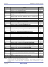
CHAPTER 22 SAFETY FUNCTIONS
p.772 Modification of (6) Frequency detection function (c)
p.775
Modification of Figure 22-3. Flowchart of Flash Memory CRC Operation Function (High-
speed CRC)
(c)
p.779, 780 Modification of Figures 22-8 and 22-9 (c)
p.782 Modification of Figure 22-11. Invalid Access Detection Area (c)
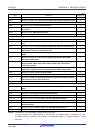
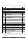
Remark “Classification” in the above table classifies revisions as follows.
(a): Error correction, (b): Addition/change of specifications, (c): Addition/change of description or note,
(d): Addition/change of package, part number, or management division, (e): Addition/change of related
documents
R01UH0305EJ0200 Rev.2.00 966
Jul 04, 2013