


RL78/G1A CHAPTER 25 FLASH MEMORY
25.8 Data Flash
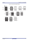
25.8.1 Data flash overview
An overview of the data flash memory is provided below.
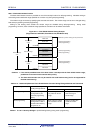
• The user program can rewrite the data flash memory by using the data flash library. For details, refer to the RL78
Family Data Flash Library User’s Manual.
• The data flash memory can also be rewritten to through serial programming using the dedicated flash memory
programmer or an external device.
• The data flash can be erased in 1-block (1 KB) units.
• The data flash can be accessed only in 8-bit units.
• The data flash can be directly read by CPU instructions.
• Instructions can be executed from the code flash memory while rewriting the data flash memory (that is, background
operation (BGO) is supported).
• Because the data flash memory is an area exclusively used for data, it cannot be used to execute instructions.
• Accessing the data flash memory is not possible while rewriting the code flash memory (during self-programming).
• Manipulating the DFLCTL register is not possible while rewriting the data flash memory.
• Transition to the STOP mode is not possible while rewriting the data flash memory.
Cautions 1. The data flash memory is stopped after a reset is canceled. The data flash control register
(DFLCTL) must be set up in order to use the data flash memory.
<R>
2. The high-speed on-chip oscillator should be kept operating during data flash rewrite. If it is kept
stopping, the high-speed on-chip oscillator clock should be operated (HIOSTOP = 0). The data
flash library should be executed after 30
μ
s have elapsed.
Remark For rewriting the code flash memory via a user program, see 25.6 Self-Programming.
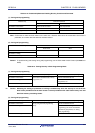
25.8.2 Register controlling data flash memory
25.8.2.1 Data flash control register (DFLCTL)
This register is used to enable or disable accessing to the data flash.
The DFLCTL register is set by a 1-bit or 8-bit memory manipulation instruction.
Reset input sets this register to 00H.
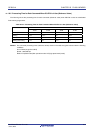
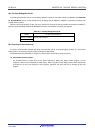
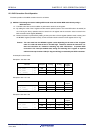
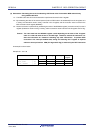
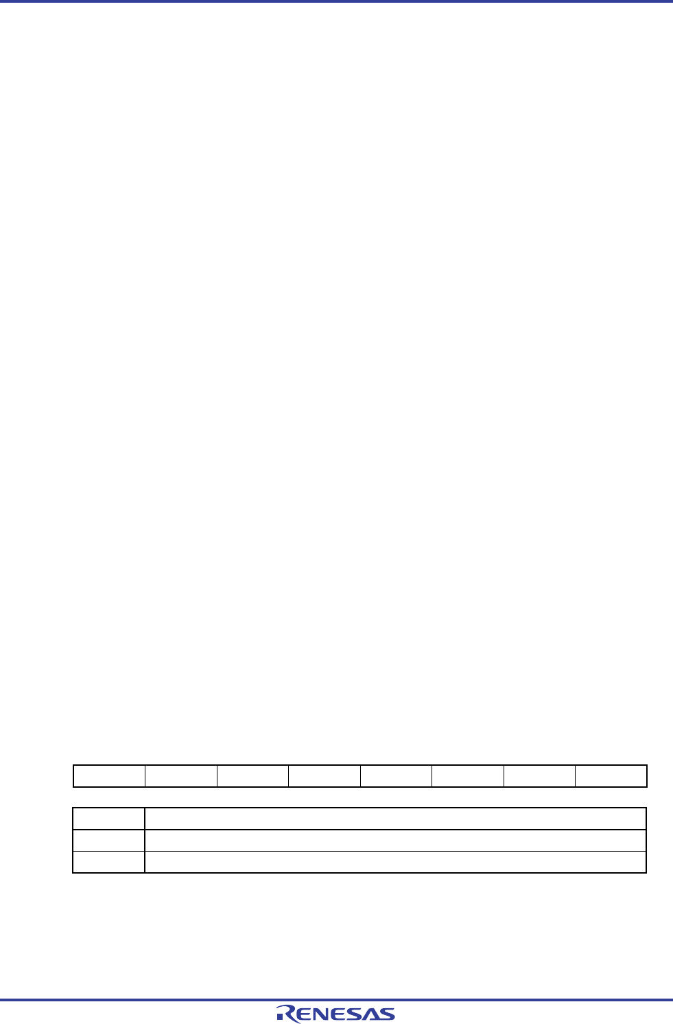
Figure 25-12. Format of Data Flash Control Register (DFLCTL)
Address: F0090H After reset: 00H R/W
Symbol 7 6 5 4 3 2 1 <0>
DFLCTL 0 0 0 0 0 0 0 DFLEN
DFLEN Data flash access control
0 Disables data flash access
1 Enables data flash access
Caution Manipulating the DFLCTL register is not possible while rewriting the data flash memory.
R01UH0305EJ0200 Rev.2.00 822
Jul 04, 2013