


RL78/G1A
CHAPTER 30 ELECTRICAL SPECIFICATIONS (G: INDUSTRIAL APPLICATIONS T
A
=
−
40 to +105
°
C)
R01UH0305EJ0200 Rev.2.00 932
Jul 04, 2013
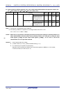
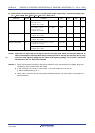
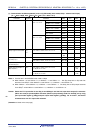
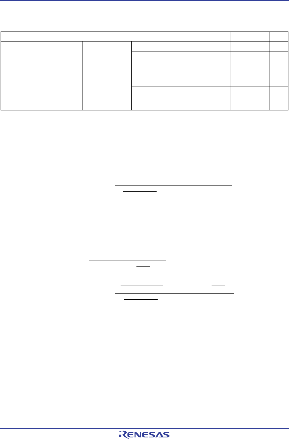
(5) Communication at different potential (1.8 V, 2.5 V) (UART mode) (dedicated baud rate generator output) (2/2)
(TA = −40 to +105°C, 2.4 V ≤ EVDD0 ≤ VDD ≤ 3.6 V, VSS = EVSS0 = 0 V)
Parameter Symbol Conditions MIN. TYP. MAX. Unit
Note 1 bps
2.7 V ≤ EVDD0 ≤ 3.6 V,
2.3 V ≤ V
b ≤ 2.7 V
Theoretical value of the maximum
transfer rate
C
b = 50 pF, Rb = 2.7 kΩ, Vb = 2.3 V
1.2
Note 2
Mbps
Note 3 bps
Transfer
rate
Transmission
2.4 V ≤ EVDD0 < 3.3 V,
1.6 V ≤ V
b ≤ 2.0 V
Theoretical value of the maximum
transfer rate
C
b = 50 pF, Rb = 5.5 kΩ, Vb = 1.6 V
0.43
Note 4
Mbps
Notes 1. The smaller maximum transfer rate derived by using f
MCK/12 or the following expression is the valid maximum
transfer rate.
Expression for calculating the transfer rate when 2.7 V ≤ EV
DD0 ≤ 3.6 V and 2.3 V ≤ Vb ≤ 2.7 V
1
Maximum transfer rate =
{−C
b × Rb × ln (1 −
2.0
Vb
)} × 3
[bps]
1
Transfer rate × 2
− {−Cb × Rb × ln (1 −
2.0
Vb
)}
Baud rate error (theoretical value) = × 100 [%]
(
1
Transfer rate
) × Number of transferred bits
* This value is the theoretical value of the relative difference between the transmission and reception sides.
2. This value as an example is calculated when the conditions described in the “Conditions” column are met.
See Note 1 above to calculate the maximum transfer rate under conditions of the customer.
3. The smaller maximum transfer rate derived by using f
MCK/12 or the following expression is the valid maximum
transfer rate.
Expression for calculating the transfer rate when 2.4 V ≤ EV
DD0 < 3.3 V and 1.6 V ≤ Vb ≤ 2.0 V
1
Maximum transfer rate =
[bps]
{−C
b × Rb × ln (1 −
1.5
Vb
)} × 3
1
Transfer rate × 2
− {−Cb × Rb × ln (1 −
1.5
V
b
)}
Baud rate error (theoretical value) = × 100 [%]
(
1
Transfer rate
) × Number of transferred bits
* This value is the theoretical value of the relative difference between the transmission and reception sides.
4. This value as an example is calculated when the conditions described in the “Conditions” column are met.
See Note 3 above to calculate the maximum transfer rate under conditions of the customer.
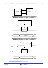
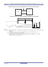
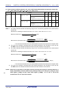
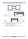
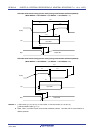
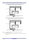
Caution Select the TTL input buffer for the RxDq pin and the N-ch open drain output (V
DD tolerance (When 25- to
48-pin products)/EV
DD tolerance (When 64-pin products)) mode for the TxDq pin by using port input
mode register g (PIMg) and port output mode register g (POMg). For V
IH and VIL, see the DC
characteristics with TTL input buffer selected.
<R>