


RL78/G1A
CHAPTER 30 ELECTRICAL SPECIFICATIONS (G: INDUSTRIAL APPLICATIONS T
A
=
−
40 to +105
°
C)
R01UH0305EJ0200 Rev.2.00 935
Jul 04, 2013
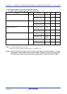
(6)
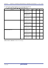
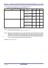
Communication at different potential (1.8 V, 2.5 V) (CSI mode) (master mode, SCKp... internal clock output) (2/2)
(TA = −40 to +105°C, 2.4 V ≤ EVDD0 ≤ VDD ≤ 3.6 V, VSS = EVSS0 = 0 V)
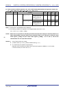
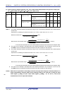
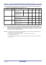
Parameter Symbol Conditions MIN. TYP. MAX. Unit
2.7 V ≤ EVDD0 ≤ 3.6 V, 2.3 V ≤ Vb ≤ 2.7 V,
C
b = 30 pF, Rb = 2.7 kΩ
354 ns
SIp setup time
(to SCKp↑)
Note 1
t
SIK1
2.4 V ≤ EV
DD0 < 3.3 V, 1.6 V ≤ Vb ≤ 2.0 V,
C
b = 30 pF, Rb = 5.5 kΩ
958 ns
2.7 V ≤ EVDD0 ≤ 3.6 V, 2.3 V ≤ Vb ≤ 2.7 V,
C
b = 30 pF, Rb = 2.7 kΩ
38 ns
SIp hold time
(from SCKp↑)
Note 1
t
KSI1
2.4 V ≤ EV
DD0 < 3.3 V, 1.6 V ≤ Vb ≤ 2.0 V,
C
b = 30 pF, Rb = 5.5 kΩ
38 ns
2.7 V ≤ EVDD0 ≤ 3.6 V, 2.3 V ≤ Vb ≤ 2.7 V,
C
b = 30 pF, Rb = 2.7 kΩ
390 ns
Delay time from SCKp↓ to
SOp output
Note 1
t
KSO1
2.4 V ≤ EV
DD0 < 3.3 V, 1.6 V ≤ Vb ≤ 2.0 V,
C
b = 30 pF, Rb = 5.5 kΩ
966 ns
2.7 V ≤ EVDD0 ≤ 3.6 V, 2.3 V ≤ Vb ≤ 2.7 V,
C
b = 30 pF, Rb = 2.7 kΩ
88 ns
SIp setup time
(to SCKp↓)
Note 2
t
SIK1
2.4 V ≤ EV
DD0 < 3.3 V, 1.6 V ≤ Vb ≤ 2.0 V,
C
b = 30 pF, Rb = 5.5 kΩ
220 ns
2.7 V ≤ EVDD0 ≤ 3.6 V, 2.3 V ≤ Vb ≤ 2.7 V,
C
b = 30 pF, Rb = 2.7 kΩ
38 ns
SIp hold time
(from SCKp↓)
Note 2
t
KSI1
2.4 V ≤ EV
DD0 < 3.3 V, 1.6 V ≤ Vb ≤ 2.0 V,
C
b = 30 pF, Rb = 5.5 kΩ
38 ns
2.7 V ≤ EVDD0 ≤ 3.6 V, 2.3 V ≤ Vb ≤ 2.7 V,
C
b = 30 pF, Rb = 2.7 kΩ
50 ns
Delay time from SCKp↑ to
SOp output
Note 2
t
KSO1
2.4 V ≤ EV
DD0 < 3.3 V, 1.6 V ≤ Vb ≤ 2.0 V,
C
b = 30 pF, Rb = 5.5 kΩ
50 ns
Notes 1. When DAPmn = 0 and CKPmn = 0, or DAPmn = 1 and CKPmn = 1.
2. When DAPmn = 0 and CKPmn = 1, or DAPmn = 1 and CKPmn = 0.
Caution Select the TTL input buffer for the SIp pin and the N-ch open drain output (V
DD tolerance (When 25- to
48-pin products)/EV
DD tolerance (When 64-pin products)) mode for the SOp pin and SCKp pin by using
port input mode register g (PIMg) and port output mode register g (POMg). For V
IH and VIL, see the DC
characteristics with TTL input buffer selected.
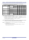
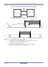
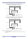
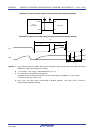
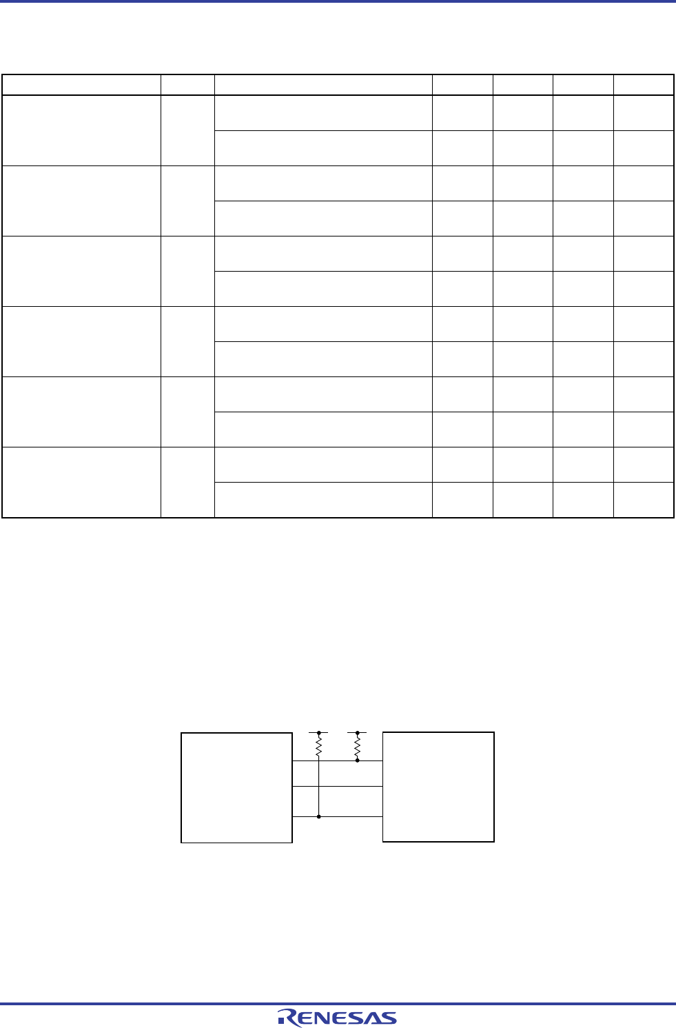
CSI mode connection diagram (during communication at different potential)
V
b
R
b
SCKp
SOp
SCK
SI
User device
SIp SO
V
b
R
b
<Master>
RL78
microcontroller
Remarks 1. Rb[Ω]: Communication line (SCKp, SOp) pull-up resistance, Cb[F]: Communication line (SCKp, SOp) load
capacitance, Vb[V]: Communication line voltage
2. p: CSI number (p = 00, 10, 20), m: Unit number , n: Channel number (mn = 00, 02, 10),
g: PIM and POM number (g = 0, 1)
3. CSI01, CSI11, and CSI21 cannot communicate at different potential. Use other CSI for communication at
different potential.
<R>