


RL78/G1A APPENDIX A REVISION HISTORY
(2/11)
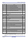
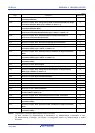
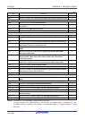
Page Description Classification
p.110 Modification of 4.3.6 Port mode control registers (PMCxx) (c)
p.111 Modification of 4.3.7 A/D port configuration register (ADPC) (c)
p.112 Modification of 4.3.8 Peripheral I/O redirection register (PIOR) (c)
p.113 Modification of 4.3.9 Global digital input disable register (GDIDIS) (c)
p.114 Modification of 4.3.10 Global analog input disable register (GAIDIS) (c)
p.116 Modification of 4.4.4 Handling different potential (1.8 V or 2.5 V) by using EVDD ≤ VDD (c)
p.116, 117 Modification of 4.4.5 Handling different potential (1.8 V or 2.5 V) by using I/O buffers (c)
p.118 Modification of 4.5 Register Settings When Using Alternate Function (c)
p.119
Modification of 4.5.2 Register settings for alternate function whose output function is not
used
(c)
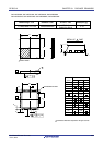
p.120 Modification of 4.5.3 Register setting examples for used port and alternate functions (c)
p.121 to 136
Modification of Table 4-6. Setting Examples of Registers and Output Latches When
Using Alternate Function
(c)
p.138 Modification of 4.6.2 Notes on specifying the pin settings (c)
CHAPTER 5 CLOCK GENERATOR
p.140 Modification of (3) Low-speed on-chip oscillator clock (Low-speed on-chip oscillator) (c)
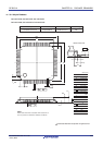
p.141 Modification of Table 5-1. Configuration of Clock Generator (c)
p.142 Modification of Figure 5-1. Block Diagram of Clock Generator (c)
p.143 Modification of 5.3 Registers Controlling Clock Generator (c)
p.145 Modification of Caution 7 (c)
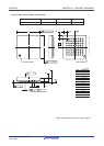
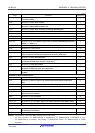
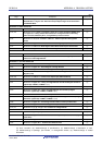
p.149
Modification of Figure 5-5. Format of Oscillation Stabilization Time Counter Status
Register (OSTC)
(c)
p.150 Modification of 5.3.5 Oscillation stabilization time select register (OSTS) (c)
p.151
Modification of Figure 5-6. Format of Oscillation Stabilization Time Select Register
(OSTS)
(c)
p.155 Modification of 5.3.7 Subsystem clock supply mode control register (OSMC) (c)
p.156 Modification of 5.3.8 High-speed on-chip oscillator frequency select register (HOCODIV) (c)
p.159 Modification of Caution in Figure 5-12. Example of External Circuit of XT1 Oscillator (c)
p.162 Modification of 5.4.4 Low-speed on-chip oscillator (c)
p.167 Modification of 5.6.3 Example of setting XT1 oscillation clock (c)
p.170 to 173 Modification of Table 5-3. CPU Clock Transition and SFR Register Setting Examples (c)
p.174
Modification of 5.6.5 Condition before changing CPU clock and processing after
changing CPU clock
(c)
p.178 Modification of Figure 5-16. External Oscillation Circuit Example (c)
p.181 Modification of (1) X1 oscillation and (2) XT1 oscillation (c)
CHAPTER 6 TIMER ARRAY UNIT
p.185 Modification of 6.1.2 Simultaneous channel operation function (c)
p.188 Modification of Table 6-1. Configuration of Timer Array Unit (c)
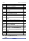
p.191
Modification of Figure 6-3. Internal Block Diagram of Channels 1 and 3 of Timer Array
Unit 0
(c)
p.197 Modification of Figure 6-9. Format of Peripheral Enable Register 0 (PER0) (c)
Remark “Classification” in the above table classifies revisions as follows.
(a): Error correction, (b): Addition/change of specifications, (c): Addition/change of description or note,
(d): Addition/change of package, part number, or management division, (e): Addition/change of related
documents
R01UH0305EJ0200 Rev.2.00 959
Jul 04, 2013