


RL78/G1A CHAPTER 11 A/D CONVERTER
R01UH0305EJ0200 Rev.2.00 361
Jul 04, 2013
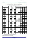
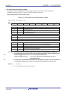
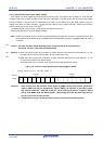
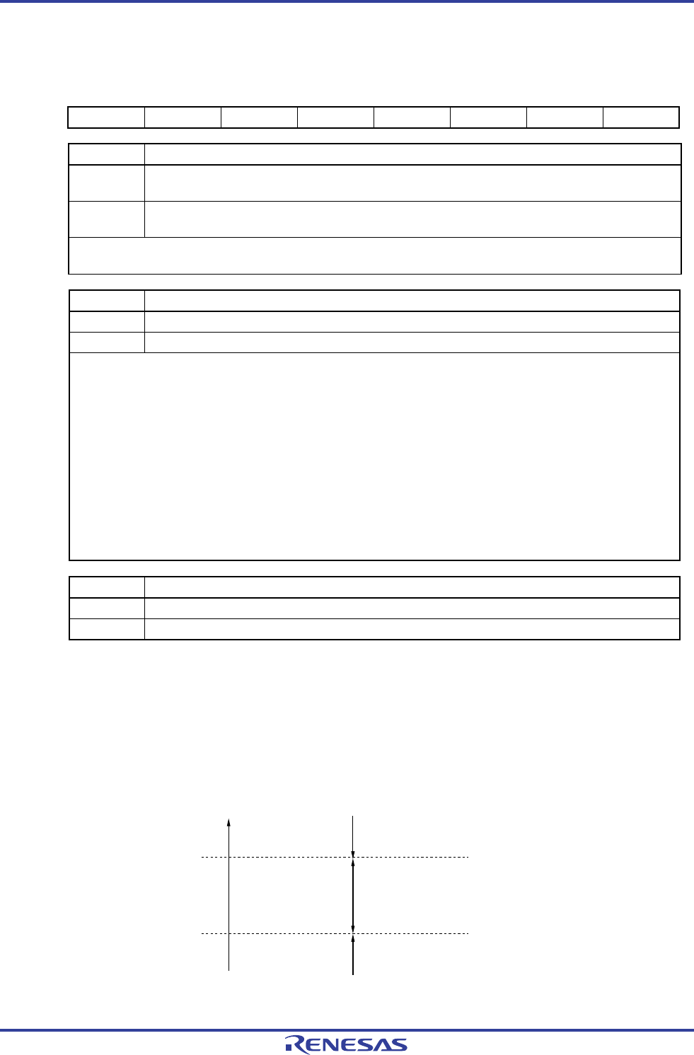
Figure 11-7. Format of A/D Converter Mode Register 2 (ADM2) (2/2)
Address: F0010H After reset: 00H R/W
Symbol 7 6 5 4 <3> <2> 1 <0>
ADM2 ADREFP1 ADREFP0 ADREFM 0 ADRCK AWC 0 ADTYP
ADRCK Checking the upper limit and lower limit conversion result values
0 The A/D conversion end interrupt request signal (INTAD) is output when the ADLL register ≤ the ADCR
register ≤ the ADUL register (AREA1).
1 The A/D conversion end interrupt request signal (INTAD) is output when the ADCR register < the ADLL
register (AREA2) or the ADUL register < the ADCR register (AREA3).
Figure 11-8 shows the generation range of the A/D conversion end interrupt request signal (INTAD) for AREA1 to
AREA3.
AWC Specification of the SNOOZE mode
0 Do not use the SNOOZE mode function.
1 Use the SNOOZE mode function.
When there is a hardware trigger signal in the STOP mode, the STOP mode is exited, and A/D conversion is performed
without operating the CPU (the SNOOZE mode).
• The SNOOZE mode function can only be specified when the high-speed on-chip oscillator clock is selected for the
CPU/peripheral hardware clock (f
CLK). If any other clock is selected, specifying this mode is prohibited.
• Using the SNOOZE mode function in the software trigger mode or hardware trigger no-wait mode is prohibited.
• Using the SNOOZE mode function in the sequential conversion mode is prohibited.
• When using the SNOOZE mode function, specify a hardware trigger interval of at least “shift time to SNOOZE
mode
Note 1
+ A/D power supply stabilization wait time + A/D conversion time +2 fCLK clock”
• Even when using SNOOZE mode, be sure to set the AWC bit to 0 in normal operation and change it to 1 just before
shifting to STOP mode.
Also, be sure to change the AWC bit to 0 after returning from STOP mode to normal operation.
If the AWC bit is left set to 1, A/D conversion will not start normally in spite of the subsequent SNOOZE or normal
operation.
ADTYP Selection of the A/D conversion resolution
0 12-bit resolution
Note 2
1 8-bit resolution
Notes 1. Refer to “Transition time from STOP mode to SNOOZE mode:” in 18.3.3 SNOOZE mode
2. The valid resolution differs depending on the voltage conditions of AV
DD and AVREFP.
For details, see 29.6.1 A/D converter characteristics.
Caution Rewrite the value of the ADM2 register while conversion operation is stopped (ADCS = 0, ADCE = 0).
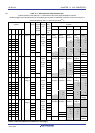
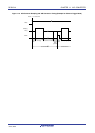
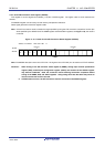
Figure 11-8. ADRCK Bit Interrupt Signal Generation Range
111111111111B
000000000000B
ADCR register value
(A/D conversion result)
AREA 1
(ADLL ≤ ADCR ≤ ADUL)
AREA 2
(ADCR < ADLL)
AREA 3
(ADUL < ADCR)
ADUL register setting
INTAD is generated
when ADRCK = 0.
INTAD is generated
when ADRCK = 1.
INTAD is generated
when ADRCK = 1.
ADLL register setting
Remark If INTAD does not occur, the A/D conversion result is not stored in the ADCR or ADCRH register.
<R>
<R>
<R>