


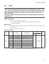

85
CHAPTER 4 I/O PORTS
4.4.2 Operation of Port 2
This section describes the operations of the port 2.
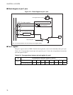
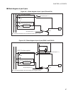
■ Operation of port 2
●
Operation as an output port
• Writing data to the PDR2 register stores the data in the output latch. When the output latch value is "0",
the output transistor turns "ON" and an "L" level is output from the pin. When the output latch value is
"1", the transistor turns "OFF" and high impedance (Hi-Z) is output from the pin.
• Reading the PDR2 register returns the output latch value.
●
Operation as an input port
• Writing "0" to the PDR2 register set the port as an input port, the output transistor is "OFF" and the pin
goes to the high-impedance state.
• Reading the PDR2 register returns the pin value.
●
Operation as an LCD segment driver output
• When the LCD output mask option is selected, set the PDR2 register bits corresponding to the LCD
segment driver output pins to "1" to turn the output transistor "OFF".
• You cannot read the LCD output data by reading PDR2.
●
Operation at reset
• Resetting the CPU initializes the PDR2 register values to "1". This turns "OFF" the output transistor for
all pins and all pins are in high-impedance (Hi-Z) state.
●
Operation in stop mode
• The output transistors are forcibly turned "OFF" and the pins go to the high-impedance state if the pin
state specification bit in the standby control register (STBC: SPL) is "1" when the device goes to stop
mode.
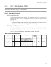
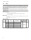
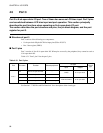
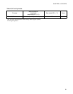
Table 4.4-4 "Port 2 pin state" lists the port 2 pin states.
Table 4.4-4 Port 2 pin state
Pin name
Normal operation
sleep mode
stop mode (SPL = "0")
Stop mode (SPL = "1") Reset
P20/SEG36 to P25/SEG41
General-purpose I/O ports/segment
driver output
Hi-Z Hi-Z
SPL: Pin state specification bit in the standby control register (STBC)
Hi-Z: High impedance