


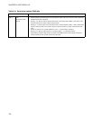
174
CHAPTER 9 8-BIT SERIAL I/O
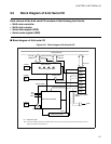
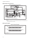
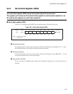
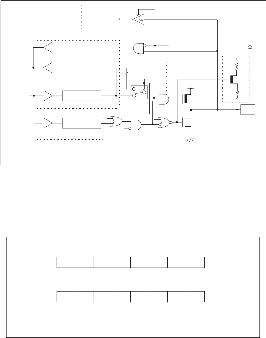
■ Block diagram of 8-bit serial I/O pins
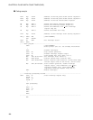
Figure 9.3-1 Block diagram of 8-bit serial I/O pin
Reference:
Pins with a pull-up resistor go to the "H" level (pull-up state) rather than to the high-impedance state
when the output transistor is turned "OFF".
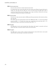
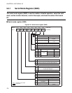
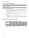
■ 8-bit serial I/O registers
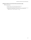
Figure 9.3-2 8-bit serial I/O registers
PDR (Port data register)
DDR
Internal data bus
PDR read
PDR read
Output latch
PDR write
DDR write
Pin
SPL: Pin state specification bit in the standby control register (STBC)
N-ch
Stop mode (SPL = 1)
To SIO input
(Port data direction register)
SIO output
SIO
output enable
P-ch
Pull-up resistor
Approx. 50 k
P-ch
(When Read-modify-write instruction executed)
Stop mode (SPL = 1)
(Mask option)
For P43/SI and P45/SCK
P43/SI
P44/SO
P45/SCK
P44/SO
P45/SCK
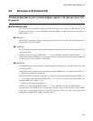
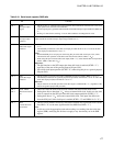
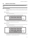
SMR (Serial mode register)
SDR (Serial data register)
Address Bit 7 Bit 6 Bit 5 Bit 4 Bit 3 Bit 2 Bit 1 Bit 0 Initial value
001C
H
SIOF SIOE SCKE SOE CKS1 CKS0 BDS SST 00000000
B
R/W R/W R/W R/W R/W R/W R/W R/W
Address Bit 7 Bit 6 Bit 5 Bit 4 Bit 3 Bit 2 Bit 1 Bit 0 Initial value
001D
H
XXXXXXXX
B
R/W R/W R/W R/W R/W R/W R/W R/W
R/W : Readable and writable
X : Indeterminate