


226
CHAPTER 11 EXTERNAL INTERRUPT CIRCUIT (EDGE)
11.3 Structure of the External Interrupt Circuit
This section describes the pins, pin block diagram, register, and interrupt sources of
the external interrupt circuit.
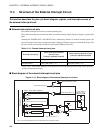
■ External interrupt circuit pins
The external interrupt circuit has two external interrupt pins.
The external interrupt pins can function either as external interrupt inputs (hysteresis inputs) or general I/O
ports.
Although the P42/PWC/INT1 and P46/INT0 pins continuously function as external interrupt inputs, the
external interrupt circuit does not output interrupts if output of interrupt requests is disabled for the pin. The
pin states can be read directly from the port data register (PDR4) at any time.
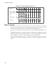
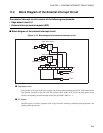
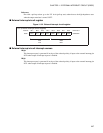
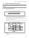
■ Block diagram of the external interrupt circuit pins
Figure 11.3-1 Block diagram of the external interrupt circuit pins
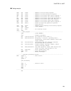
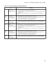
Table 11.3-1 External interrupt circuit pins
External interrupt pin
When used as an external
interrupt input
(interrupt requests enabled)
When used as general I/O port
(interrupt requests disabled)
P46/INT0 INT0 (EIC: EIE0 = "1") P46 (EIC: EIE0 = "0")
P42/PWC/INT1 INT1 (EIC: EIE1 = "1") P42 (EIC: EIE1 = "0")
INT0 - INT1: The external interrupt circuit generates the interrupt request when an edge of the specified
polarity is detected on the pin.
PDR (Port data register)
DDR
Internal data bus
PDR read
PDR read
Output latch
PDR write
DDR write
Pin
N-ch
Stop mode (SPL = 1)
(Port data direction register)
P-ch
Pull-up resistor
Approx. 50 k
P-ch
(When Read-modify-write instruction executed)
Stop mode (SPL = 1)
To external interrupt
External interrupt enable
(Mask option)
SPL: Pin state specification bit in the standby control register (STBC)