


126
CHAPTER 7 8-BIT PWM TIMER
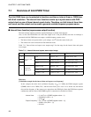
7.3 Structure of 8-bit PWM Timer
This section describes the pin, pin block diagram, register source, and interrupts of the
8-bit PWM timer.
■ 8-bit PWM timer pin
The 8-bit PWM timer uses the P41/PWM pin. This pin can function as a CMOS general-purpose I/O port
(P41), or as the interval timer or PWM timer output (PWM).
PWM: When the interval timer function is selected, the square waves are output to this pin.
When the PWM timer function is selected, the pin outputs the PWM wave.
Setting the output pin control bit (CNTR: OE) to "1" makes pin P41/PWM the output-only pin for 8-bit
PWM timer. Once this has been done, the pin performs its PWM function regardless of the state of the port
data register output latch data (PDR4: bit 1).
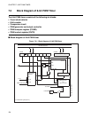
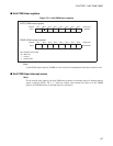
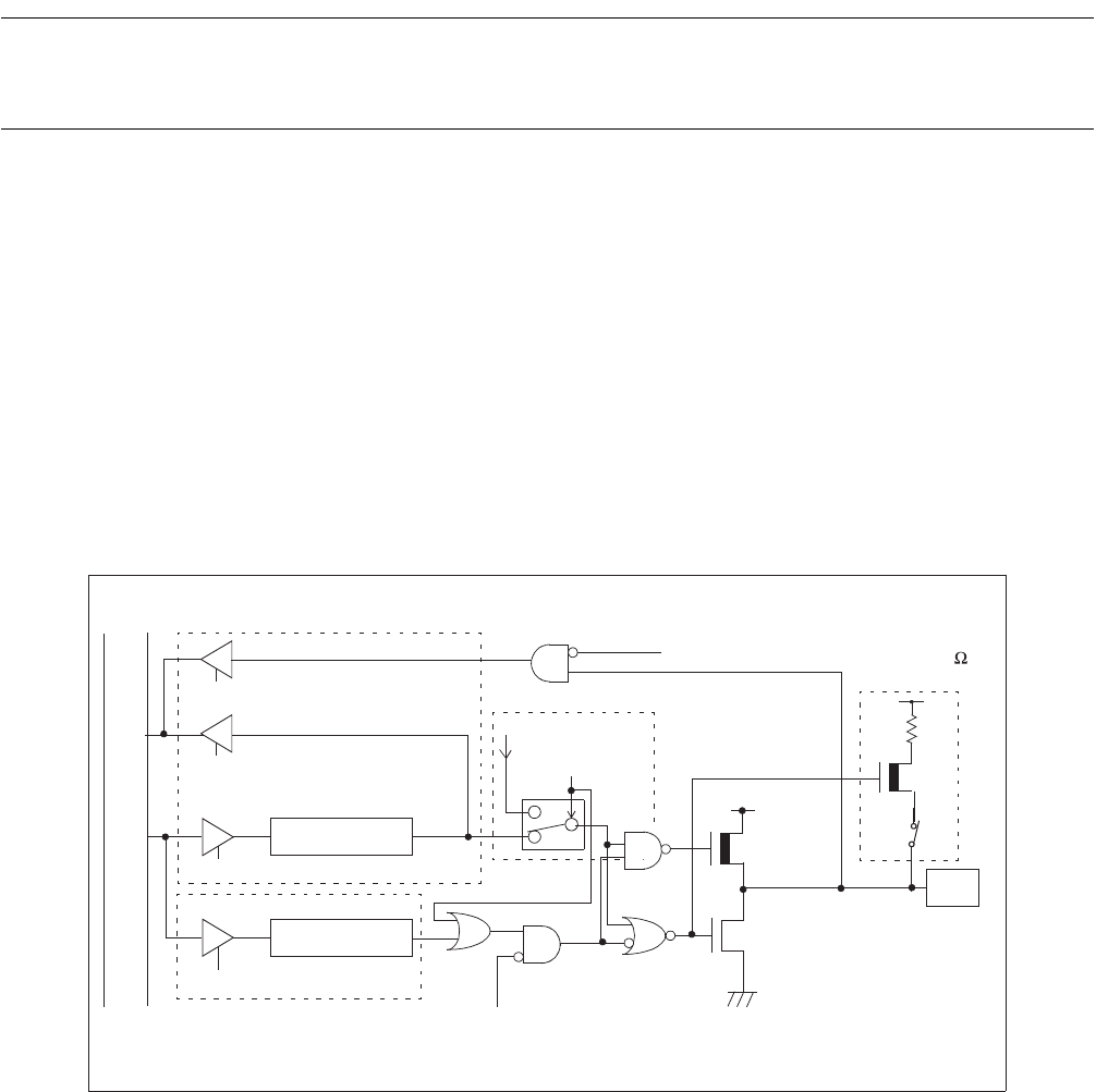
■ Block diagram of 8-bit PWM timer pin
Figure 7.3-1 Block diagram of 8-bit PWM timer pin
PDR (Port data register)
DDR
Internal data bus
PDR read
PDR read
Output latch
PDR write
DDR write
Pin
SPL: Pin state specification bit in the standby control register (STBC)
N-ch
Stop mode (SPL = 1)
(Port data direction register)
PWM output
PWM
output enable
P-ch
Pull-up resistor
Approx. 50 k
P-ch
(When Read-modify-write instruction executed)
Stop mode (SPL = 1)
(Mask option)
P41/PWM