


202
CHAPTER 10 UART
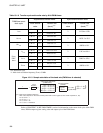
10.3 UART Pins
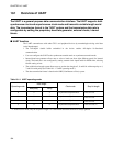
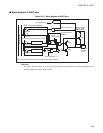
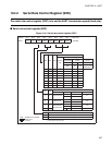
This section describes the pins and pin block diagram of UART.
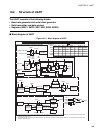
■ UART pins
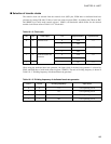
The pins for the UART function are shift clock input/output pin (P45/SCK), serial data output pin (P44/SO)
and serial data input pin (P43/SI).
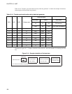
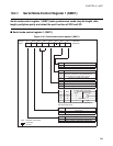
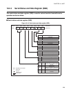
P45/SCK:
This pin function either as a general-purpose input/output port (P45) or a clock input output pin
(hysteresis input) for the UART(SCK).
When clock output is enabled (SMC1: SCKE = "1"), this pin functions as clock output pin (SCK)
irrespective of settings on corresponding port direction register. In this case, do not select an external
clock (SRC: CS1, CS0 are not "00
B
").
To use the port as a UART clock input pin, disable the clock output (SMC1: SCKE = "0") and
configure the port as an input port by setting a corresponding port direction register bit (DDR4: bit 5 =
"0"). In this case, be sure to select an external clock (SRC: CS1, CS0 = "00
B
").
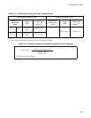
P44/SO:
This pin functions either as general-purpose input/output port (P44) or serial data output pin of the
UART (SO).
When serial data output is enabled (SMC1: SOE = "1"), this pin functions as serial data output pin of
the UART irrespective of settings on corresponding port direction register.
P43/SI:
This pin functions either as general-purpose input/output port (P43) or serial data input pin of the
UART (SI).
To use the port as a UART serial data input pin, configure the port as output port by setting a
corresponding bit of the port data direction register (DDR4: bit 3 = "0").