


192
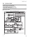
CHAPTER 9 8-BIT SERIAL I/O
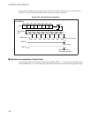
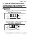
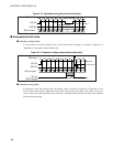
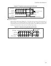
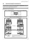
■ Program example for serial input
●
Processing description
• Inputs 8-bit serial data from the SI pin of serial I/O, then generates an interrupt when transfer is
completed.
• The interrupt processing routine reads the transferred data and continues transfer.
• Serial I/O uses the external shift clock. The shift clock is input from the SCK pin.
●
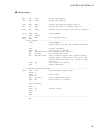
Coding example
DDR4 EQU 000FH
SMR EQU 001CH ; Serial mode register
SDR EQU 001DH ; Serial data register
SIOF EQU SMR:7 ; Define the interrupt request flag bit.
SST EQU SMR:0 ; Define the serial I/O transfer start bit.
ILR2 EQU 007DH ; Address of the interrupt level setting register 2
INT_V DSEG ABS ; [DATA SEGMENT]
ORG 0FFF0H
IRQ5 DW WARI ; Set interrupt vector.
INT_V ENDS
;-----Main program----------------------------------------------------------------
CSEG ; [CODE SEGMENT]
; Stack pointer (SP) etc. are already initialized.
:
MOV DDR4,#00000000B ; Set P45/SCK and P43/SI pin as an input.
CLRI ; Disable interrupts.
CLRB SST ; Stop serial I/O transfer.
MOV ILR2,#11110111B ; Set interrupt level (level 1).
MOV SMR,#01001100B ; Clear interrupt request flag, enable interrupt
; request output, set shift clock input (SCK),
; disable serial data output (SO), select the
; external shift clock, LSB first.
SETB SST ; Enable serial I/O transfer.
SETI ; Enable interrupts.
:
;---------------------------------------------------------------------------------
WARI CLRB SIOF ; Clear interrupt request flag.
PUSHW A
XCHW A,T
PUSHW A
MOV A,SDR ; Read transfer data.
SETB SST ; Enable serial I/O transfer.
:
User processing
:
POPW A
XCHW A,T
POPW A
RETI
ENDS
;---------------------------------------------------------------------------------
END