


241
CHAPTER 12 LCD CONTROLLER/DRIVER
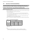
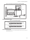
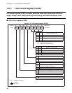
12.3 Structure of LCD Controller/Driver
This section describes the pins, pin block diagrams, registers, and display RAM of the
LCD controller/driver.
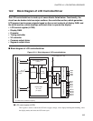
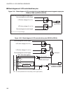
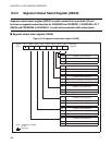
■ LCD controller/driver pins
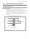
The LCD controller/driver uses 4 common output pins (COM0 to COM3), 42 segment output pin (SEG0 to
SEG41), and 3 LCD driving power supply pins (V1 to V3).
●
COM0, COM1, COM2, and COM3 pins
COM0 to COM3 can function LCD common output pins (COM0 to COM3).
●
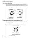
SEG0 to SEG19, P00/SEG20 to P07/SEG27, P10/SEG28 to P17/SEG35 and P20/SEG36 to P25/
SEG41
P00/SEG20 to P07/SEG27, P10/SEG28 to P17/SEG35 and P20/SEG36 to P25/SEG41 pins can function
either as N-ch open-drain I/O ports (P00 to P07, P10 to P17 and P20 to P25) and LCD segment output pins
(SEG20 to SEG41). The selection, however is made as a mask option.
Note:
When these pins are used as LCD segment outputs, the corresponding port data registers (PDR0, PDR1
and PDR2) should be set to all "1" to turn the output transistors "OFF".
●
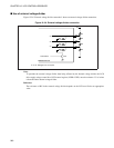
P32/V1, P33/V2 and V3
V1, V2 and V3 pins are the LCD driving power supply pins. The P32/V1 and P33/V2 can function either as
N-ch open-drain I/O ports (P32 and P33) and LCD driving power supply pins (V1 and V2). The selection,
however is made by setting LCDR: PSEL bit.