


95
CHAPTER 4 I/O PORTS
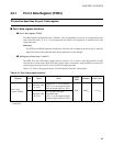
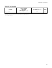
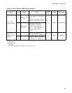
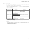
Table 4.6-3 Port 4 PDR and DDR register function
Register Data Read Write
Read/
Write
Address Initial value
Port 4 data
register (PDR4)
0
Pin state is the
"L" level.
Outputs an "L" level to the pin if
the pin functions as an output
port.
(Sets "0" to the output latch and
turns the output transistor "ON".)
R/W
000E
H
-XXXXXXX
B
1
Pin state is the
"H" level.
Sets the pin to the high-
impedance state if the pin
functions as an output port.
(*)
(Sets "1" to the output latch and
turns the output transistor
"OFF".)
Port 4 data
direction register
(DDR4)
0--
Disables the output transistor
and sets the pin as an input pin.
W
000F
H
-0000000
B
1--
Enables the output transistor and
sets the pin as an output pin.
R/W: Readable and writable
W: Write-only
X: Indeterminate
-: Unused bit
*: Pins with a pull-up resistor (optional), go to the "H" level