


250
CHAPTER 12 LCD CONTROLLER/DRIVER
12.4 Operation of LCD Controller/Driver
The LCD controller/driver provides the necessary control and drive for an LCD.
■ Operation of LCD controller/driver
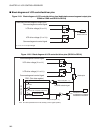
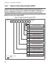
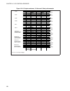
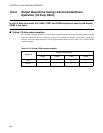
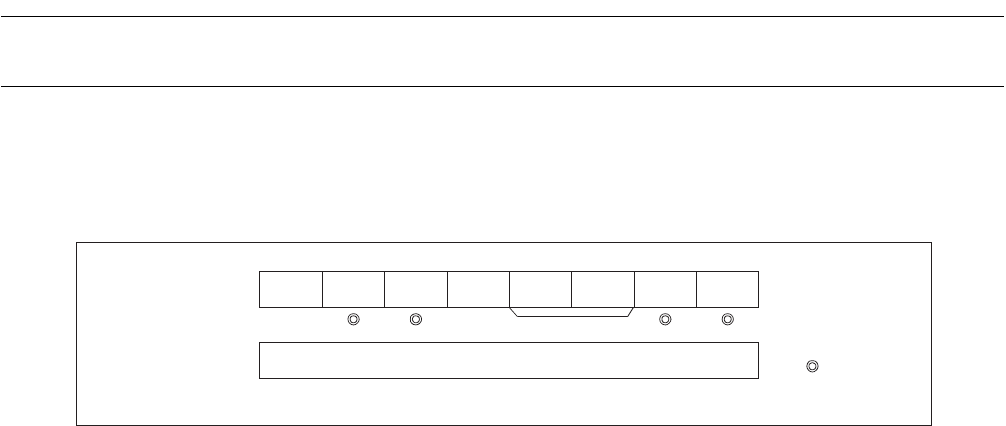
Figure 12.4-1 "LCD controller/driver settings" shows the settings required to operate the LCD.
Figure 12.4-1 LCD controller/driver settings
Once the above settings have been made, if the selected clock for frame cycle generation is running, LCD
panel driving waveforms reflecting the contents of display RAM will be output at the segment and common
output pins (COM0 to COM3 and SEG0 to SEG42).
Although the clock for frame period generation can be switched even while the LCD is displaying data, the
display may flicker when the switching occurs. This can be avoided by temporarily blanking the display
(LCDR: BK = "1"), etc. while switching.
The display driving output is a two-frame a.c. waveform for which the bias level and display duty cycle is
selected by settings.
When LCD operation is stopped (LCDR: MS1, MS0 = "00
B
"), and during reset, all COM and SEG output
pins are pulled "L" state so that nothing is displayed on the LCD panel.
Note:
If the selected frame cycle generate clock were to stop while the LCD is operating, the circuit that
converts the waveform from d.c. to a.c. would also stop, causing a d.c. voltage to be applied to the
liquid crystal cells. The LCD must therefore be stopped before the clock is stopped. The conditions
under which the main clock is stopped is a function of the clock mode and standby mode.
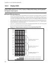
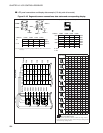
■ LCD driving waveforms
It is characteristic of LCD that applying d.c. drive to the panel can cause electrochemical degradation of the
material used in the LCD cells. For this reason, the LCD controller/driver includes a circuit to convert the
original driving waveform to a two-frame a.c. output waveform (zero d.c. bias) to drive the LCD. There are
three types of output waveform:
• 1/2 bias, 1/2 duty ratio output waveform
• 1/3 bias, 1/3 duty ratio output waveform
• 1/3 bias, 1/4 duty ratio output waveform
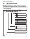
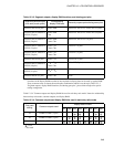
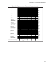
Bit 7 Bit 6 Bit 5 Bit 4 Bit 3 Bit 2 Bit 1 Bit 0
LCDR RESV PSEL VSEL BK MS1 MS0 FP1 FP0
0
0
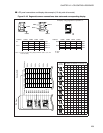
Display RAM
064
H
to 078
H
Display data
: Used bit
1 : Set "1"
0 : Set "0"
Other than "00B"