


244
CHAPTER 12 LCD CONTROLLER/DRIVER
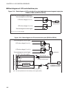
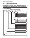
12.3.1 LCD Control Register (LCDR)
LCD control register (LCDR) is used to select the frame cycle, control the LCD drive
supply voltage, select display blanking/non-blanking, and select the display mode.
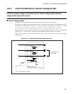
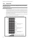
■ LCD control register (LCDR)
Figure 12.3-5 LCD control register (LCDR)
Address Bit 7 Bit 6 Bit 5 Bit 4 Bit 3 Bit 2 Bit 1 Bit 0 Initial value
0079
H
RESV PSEL VSEL BK MS1 MS0 FP1 FP0 -0010000
B
R/W R/W R/W R/W R/W R/W R/W R/W
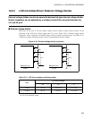
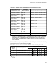
FP1 FP0
Frame cycle selection bits
Display mode selection bits
Display blanking selection bit
Drive supply voltage control bit
LCD voltage supply selection bit
Reserved bit
0 0
F
CH
/(2
11
x
x
x
x
N)
(610 Hz)
01
F
CH
/(2
12
N)
(305 Hz)
10
F
CH
/(2
13
N)
(152 Hz)
11
F
CH
/(2
14
N)
(76 Hz)
( ) : Values for F
CH
=5 MHz, and N=4
N : Number of time divisions
F
CH
: Main clock frequency oscillation
MS1 MS0
0 0
Stops LCD operation
01
1/2 duty ratio output mode (time division N = 2)
10
1/3 duty ratio output mode (time division N = 3)
11
1/4 duty ratio output mode (time division N = 4)
BK
0 Displays unblanked
1 Displays blanked
VSEL
0
Uses external voltage divider
(internal voltage divider is isolated).
1 Uses internal voltage divider.
PSEL
0 Selects as LCD power supply pins (V1 and V2)
1 Selects as port pins ( P32 and P33)
RESV
Always write
“0” to this bit.
R/W : Readable and writable
: Unused
: Initial value