


32
CHAPTER 3 CPU
3.2.2 Register Bank Pointer (RP)
The register bank pointer (RP) located in the upper 8 bits of the program status (PS)
indicates the address of the general-purpose register bank currently in use. The RP is
converted to form the actual address in general-purpose register addressing.
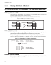
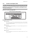
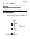
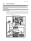
■ Structure of register bank pointer (RP)
Figure 3.2-4 "Structure of register bank pointer" shows the structure of the register bank pointer.
Figure 3.2-4 Structure of register bank pointer
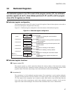
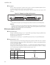
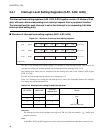
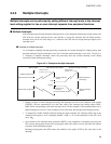
The register bank pointer indicates the address of the register bank currently in use. Figure 3.2-5 "Rule for
conversion of actual addresses of general-purpose register area" shows the relationship between the pointer
contents and the actual address is based on the conversion rule.
Figure 3.2-5 Rule for conversion of actual addresses of general-purpose register area
The register bank pointer points to the memory block (register bank) in the RAM area that is used for
general-purpose registers. A total of 32 register banks are available. A register bank is specified by setting a
value between 0 and 31 in the upper 5 bits of the register bank pointer. Each register bank contains eight 8-
bit general-purpose registers. Registers are specified by the lower 3 bits of the operation codes.
Using the register bank pointer, the addresses 0100
H
to 01FF
H
can be used as the general-purpose register
area. However, the available area is limited on some products if internal RAM only is used. The initial
value after a reset is indeterminate.
Note:
The register bank pointer is part of the program status (PS) and cannot be accessed independently.
Bit 15Bit 14 Bit 13 Bit 12 Bit 11 Bit 10 Bit 9 Bit 8 Bit 7 Bit 6 Bit 5 Bit 4 Bit 3 Bit 2 Bit 1 Bit 0
R4 R3 R2 R1 R0 ——— HIIL1IL0NZVC
RP initial value
XXXXXXXX
B
RP CCR
PS
X: Indeterminate
- : Unused
A15 A14 A13 A12 A10 A11 A9 A8 A7 A6 A5 A4 A3 A2 A1 A0
"0" "0" "0" "0" "0" "0" "0" "1" R4 R3 R2 R1 R0 b2 b1 b0
Upper bits of RP Lower operation codes
Generated addresses