


89
CHAPTER 4 I/O PORTS
4.5.1 Port 3 Data Register (PDR3)
This section describes the port 3 data register.
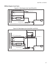
■ Port 3 data register functions
●
Port 3 data register (PDR3)
The PDR3 register holds the pin states. Therefore, a bit corresponding to a pin set as an output port can be
read as the same state ("0" or "1") as the output latch, but when it is an input port, it cannot be read as the
output latch state.
Reference:
For SETB and CLRB bit operation instructions, since the state of output latch (not the pin) is read, the
output latch states of bits other than those being operated on are not changed.
●
Settings as an bias input V1 and V2
The PSEL bit in the LCD control register must be cleared to "0" in order to select P32 and P33 as LCD
controller bias voltage input. When LCD bias voltage input is selected by using the PSEL bit in the LCD
control register, these ports can be used as LCD bias voltage input only.
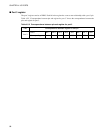
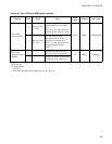
Table 4.5-3 "Port 3 data register function" lists the functions of the port 3 data register.
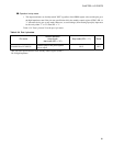
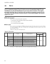
Table 4.5-3 Port 3 data register function
Register Data Read Write
Read/
Write
Address Initial value
Port 3 data
register (PDR3)
0
Pin state is the
"L" level.
Outputs an "L" level to the pin.
(Sets "0" to the output latch and
turn the output transistor "ON".)
R/W
000C
H
----1111
B
1
Pin state is the
"H" level.
Sets the pin to the high-
impedance state.
(Sets "1" to the output latch and
turn the output transistor "OFF".)
R/W: Readable and writable
-: Unused bit