


242
CHAPTER 12 LCD CONTROLLER/DRIVER
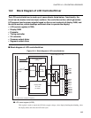
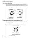
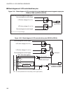
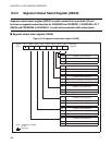
■ Block diagrams of LCD controller/driver pins
Figure 12.3-1 Block diagram of LCD controller/driver pins (dedicated common/segment output pins
COM0 to COM3 and SEG0 to SEG19)
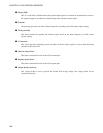
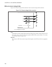
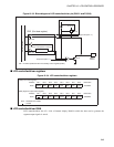
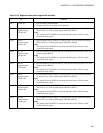
Figure 12.3-2 Block diagram of LCD controller/driver pins (SEG20 to SEG41)
Dedicated common/segment output pins
Pin
COM0 to COM3
SEG0 to SEG19
Common/segment control signal
LCD drive voltage (V
3 or V2)
LCD drive voltage (V
1 or Vss)
Common/segment control signal
V
1
to V
3
: V1 to V3 pin voltages
N-ch
P-ch
P-ch
N-ch
PDR (Port data register)
Internal data bus
PDR read (for bit manipulation instructions)
PDR write
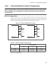
Pin
N-ch
Stop mode (SPL = 1)
SPL: Pin state specification bit in the standby control register (STBC)
PDR read
Stop mode (SPL = 1)
Mask option
Output latch
Common/segment control signal
LCD drive voltage (V
3 or V2)
LCD drive voltage (V
1 or Vss)
Common/segment control signal
N-ch
P-ch
P-ch
N-ch
Port/SEG selection signal
P00/SEG20 to P07SEG27
P10/SEG28 to P17/SEG35
P20/SEG36 to P25/SEG41