


295
APPENDIX E MB89950/950A Series Pin States
APPENDIX E MB89950/950A Series Pin States
This section describes the pin states of the MB89950/950A series in various modes.
■ MB89950/950A series pin states
The state of each pin of the MB89950/950A series of microcontrollers at sleep, stop and reset is as follows:
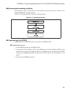
1. Sleep: The pin state immediately before entering sleep mode is held.
2. Stop: The pin state immediately before entering stop mode is held when the stop mode is started and bit
5 of the standby control register (STBC) is set to "0". When this bit is "1", outputs go to Hi-Z (High
impedance) and input/output pins go High.
3. Reset: All I/O go to Hi-Z and peripheral pins (excluding pins for pull-up option) go "H" level.
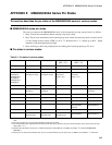
■ Pin states in various modes
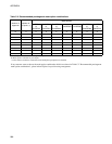
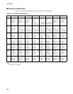
Table E-1 Pin states in various modes
Pin name Normal operation Sleep mode Stop mode
(SPL = "0")
Stop mode
(SPL = "1")
During reset
COM0 to COM3 COM outputs COM outputs Low level outputs Low level outputs Low level outputs
SEG0 to SEG19 Segment outputs Segment outputs Low level outputs Low level outputs Low level outputs
P00/SEG20 to
P07/SEG27
P10/SEG28 to
P17/SEG35
P20/SEG36 to
P25/SEG41
Port I/O
/ Peripheral output
Port I/O
/ Peripheral output
Port I/O
/ Peripheral
output = Low
High impedance
(*1)
/
Peripheral
output = Low
High impedance
(*1)
X0 Input for oscillation Input for oscillation
High impedance
(*1)
High impedance
(*1)
Input for oscillation
X1 Output for
oscillation
Output for
oscillation
High output High output Output for
oscillation
MODA Mode input Mode input Mode input Mode input Mode input
RST
Reset input Reset input Reset input Reset input
Reset input
(*2)
P30, P31 Port I/O Port I/O Port I/O
High impedance
(*1)
High impedance
P32/V1, P33/V2 Port/LCD bias Port/LCD bias Port/LCD bias
High impedance
(*4)
/
LCD bias
High impedance
(*5)
V3 Input Input Input Input Input
P40 to P46/INT0 Port I/O
/Peripheral I/O
Port I/O
/Peripheral I/O
Port I/O
/Peripheral I/O
High impedance
(*1, *3)
High impedance
(*1)
*1: The internal input level is fixed to prevent leakage due to open input. Pins for which the pull-up option is selected, enter the pull-up
state.
*2: The reset pin may serve as the output depending on the option setting.
*3: For P42 and P46, when edge detection for the external interrupt is selected, only the external interrupt can be input even in the stop
mode (SPL = "1").
*4: Whether the pins behave as I/O port or LCD bias depends on the PSEL bit of LCDR (see Chapter
12
"LCD CONTROLLER/
DRIVER").
*5: These pins are selected as LCD bias after reset. To turn P32 and P33 to ports after reset, set PSEL bit of LCDR to "1" afterwards.