


83
CHAPTER 4 I/O PORTS
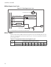
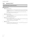
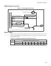
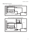
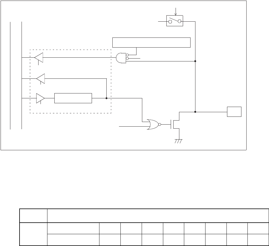
■ Block diagram of port 2 pins
Figure 4.4-1 Block diagram of port 2 pins
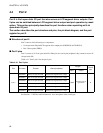
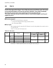
■ Port 2 register
The port 2 register consists of PDR2. Each bit in the register has a one-to-one relationship with a port 2 pin.
Table 4.4-2 "Correspondence between pin and register for port 2" shows the correspondence between the
pins and register for port 2.
PDR (Port data register)
Internal data bus
PDR read (for bit manipulation instructions)
Output latch
PDR write
Pin
N-ch
Stop mode (SPL = 1)
SPL: Pin state specification bit in the standby control register (STBC)
PDR read
Stop mode (SPL = 1)
LCD segment driver output
Mask option
Segment driver output select register
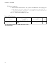
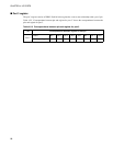
Table 4.4-2 Correspondence between pin and register for port 2
Port Correspondence between register bit and pin
Port 2
PDR2 Bit 7 Bit 6 Bit 5 Bit 4 Bit 3 Bit 2 Bit 1 Bit 0
Corresponding pin -- -- P25 P24 P23 P22 P21 P20