


90
CHAPTER 4 I/O PORTS
4.5.2 Operation of Port 3
This section describes the operations of the port 3.
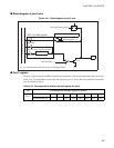
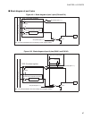
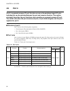
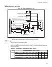
■ Operation of port 3
●
Operation as an output port
• Writing data to the PDR3 register stores the data in the output latch. When the output latch value is "0",
the output transistor turns "ON" and an "L" level is output from the pin. When the output latch value is
"1", the transistor turns "OFF" and high impedance (Hi-Z) is output from the pin.
• Reading the PDR3 register returns the output latch value.
●
Operation as an input port
• Writing "0" to the PDR3 register set the port as an input port, the output transistor is "OFF" and the pin
goes to the high-impedance state.
• Reading the PDR3 register returns the pin value.
• When V1 and V2 are selected by PSEL bit of the LCD control register, the input data is always as "0".
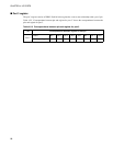
●
Operation as V1 and V2
• When V1 and V2 are selected, set the PDR3 register bits corresponding to V1 and V2 pins to "1" to turn
the output transistor "OFF".
●
Operation at reset
• At reset, these ports serve as LCD controller/driver bias input. Resetting the CPU initializes the PDR3
register values to "1". This turns "OFF" the output transistor for all pins and all pins are in high-
impedance (Hi-Z) state. Since PSEL bit of LCD control register will be reset to "0", P32 and P33 will be
configured to V1 and V2 after reset.
●
Operation in stop mode
• If P32 and P33 are selected as V1 and V2 and stop mode is entered, the voltage at those pins before
entering stop mode will be held. For port output, those pins states in stop mode are controlled by SPL bit
in the STBC register.
• The output transistors are forcibly turned "OFF" and the pins go to the high-impedance state if the pin
state specification bit in the standby control register (STBC: SPL) is "1" when the device goes to stop
mode.
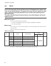
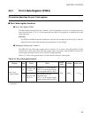
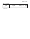
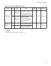
Table 4.5-4 "Port 3 pin state" lists the port 3 pin states.